Version 0.61-draft-20260105
This document is organized as successive expositions at increasing levels of detail, to give the reader an idea of the motivations and high-level differences from conventional processor architectures, eventually getting down to the detailed definitions that direct SecureRISC processor execution. So, if the introductory material seems a little vague, that is because it attempts to sketch an overall context into which the details are later fitted.
SecureRISC was created to develop old ideas and notes of mine. It is not a complete Instruction Set Architecture (ISA), but only includes the things I have had time to consider and work on. It is certainly not a specification. At present, this document exists only for discussion purposes.
The ISA is mostly just ideas at this point. The opcode assignments and
instruction specifications are little more than hints. The Virtual
Memory architecture needs work. This is not a formal specification at
this point; it is a document for discussion. Should it progress to a
specification, much rewriting would be required (e.g., to
adopt RFC 2119![]() requirement level keywords and more precise definitions.
requirement level keywords and more precise definitions.
SecureRISC began as an exploration of what a security-conscious ISA
might look like. I hope I can improve it over time to live up to its
name. Should it turn into something more than an exploration, I would
intend to make it an Open-Source ISA, along the lines
of RISC‑V![]() .
.
There is no software (simulator, compiler, operating system, etc.) for SecureRISC. This is a paper-only set of ideas at this point. A compiler, simulator, and FPGA implementation might be created at some point, but that is probably years in the future.
The reader of this document is likely already familiar with the
acronyms, terminology, and concepts used herein. Occasionally the
reader might encounter something unfamiliar. So just in case, there is
a set of glossaries at the
end of this document. Links to glossary entries are marked with a
![]() icon.
However, often links are not provided, so the reader may have to search
for unfamiliar terminology. One glossary is
for general terms used in instruction set, processor, and system software
icon.
However, often links are not provided, so the reader may have to search
for unfamiliar terminology. One glossary is
for general terms used in instruction set, processor, and system software![]() ,
with a coda to the general glossary
for terms specific to RISC‑V
,
with a coda to the general glossary
for terms specific to RISC‑V![]() that this document cites. There are also references
for programming languages
that this document cites. There are also references
for programming languages![]() , operating systems
, operating systems![]() ,
and other processor architectures
,
and other processor architectures![]() cited herein. Since cryptography terminology is used in a few places,
there is a specialized crypto glossary
cited herein. Since cryptography terminology is used in a few places,
there is a specialized crypto glossary![]() for
that. Finally,
a glossary of security vulnerabilities
for
that. Finally,
a glossary of security vulnerabilities![]() that have tripped up many processor designs
is included, since this document refers to many such things.
that have tripped up many processor designs
is included, since this document refers to many such things.
SecureRISC is an attempt to define a security-conscious Instruction Set Architecture (ISA) appropriate for server-class systems, but which, with modern process technology (e.g., 5 nm), could even be used for IoT computing given that the die area for a single such processor is a small fraction of one mm2. SecureRISC starts with the assumption that processors should enforce bounds checking and that the virtual memory system should use older, more sophisticated security measures, such as those found in Multics, including rings, segmentation, and both discretionary and mandatory (non-discretionary) access control. I also propose a new block-structured instruction set that allows for better Control Flow Integrity (CFI) and performance. For performance, several features support highly parallel execution and latency tolerance, even in implementations that avoid highly speculative execution, which can lead to security vulnerabilities.
A comment about Multics is appropriate here. There seems to be an
impression among many in the computer architecture world that many
Multics features are complex. However, they are simple and general,
easy to implement, and remove pressure on the architecture to add warts
for specialized purposes. Computer architecture from the 1980s to the
present is often an oversimplification of Multics. For example,
segmentation in Multics served to make page tables independent
of access control, which is a useful feature that has been mostly
abandoned in post-1980 architectures. Pushing access control into Page
Table Entries (PTEs) creates pressure to keep the number of bits devoted
to access control minimal when security considerations might suggest a
more robust set. Even though processor hardware has eliminated the
segment concept, operating systems (e.g., Linux) have reinvented it.
Linux calls a contiguous set of virtual pages with similar attributes
(e.g., protection)
a Virtual Memory Area (VMA)![]() .
It may be that calling it VMA instead of segments was necessary given
that a completely different usage of
.
It may be that calling it VMA instead of segments was necessary given
that a completely different usage of segmentation
terminology was
the 8086 microprocessor trying to extend its address spaces
from tiny to small![]() as an alternative to having a reasonable number of bits in a pointer.
as an alternative to having a reasonable number of bits in a pointer.
As another example, many contemporary processor architectures (e.g.,
RISC‑V) have two rings (User and Supervisor), with a single bit in
PTEs (the U bit in RISC‑V) serving as a ring bracket.
(RISC‑V has, in addition, a third ring-like privilege level called
Machine Mode, but this privilege is mostly operates without virtual
memory and so PTE bits are not needed for it.) Having only two rings
means a completely different mechanism is required for sandboxing rather
than having four rings and slightly more capable ring brackets. It was
true that rings were not well utilized on Multics, but we now have more
uses for multiple rings, such as hypervisors, Just-In-Time (JIT)
compilation, WebAssembly![]() ,
and sandboxing.
,
and sandboxing.
The goals for SecureRISC, in order of priority, are as follows:
wide issue)
Non-goals for SecureRISC include (this list will probably grow):
(An exception for low-end processor support might be a small secure enclave chip that omits floating-point, vector, and matrix operations. It might also have minimal memory translation while incorporating cryptographic features.)
Security encompasses many aspects. One of the most critical is
preventing unassisted infiltration—for example, attacks exploiting
buffer overflows, use-after-free errors, and other programming mistakes.
SecureRISC has two defenses against buffer overflows: bounds checking for
disciplined languages such
as Rust![]() and pointer/memory tagging for
undisciplined languages such as C++. Another key security issue is
unintentionally assisted infiltration, such as phishing attacks that
install Trojans. This risk may be mitigated through mandatory access
control.
and pointer/memory tagging for
undisciplined languages such as C++. Another key security issue is
unintentionally assisted infiltration, such as phishing attacks that
install Trojans. This risk may be mitigated through mandatory access
control.
The goal of SecureRISC is to provide a comprehensive security solution, but further work is required to achieve this. At present, SecureRISC focuses on areas where meaningful improvements can be made while remaining practical to implement with current processor technology.
I believe SecureRISC has yet to fully exploit the potential of mandatory access control for security, and I continue to explore opportunities in this area.
Security, garbage collection, and dynamic typing may appear to be
orthogonal, but they are synergistic. SecureRISC attempts to minimize
the impact of programming mistakes in several ways, such as making
bounds checking somewhat automatic and making compiler-generated
checking more efficient for disciplined languages where bounds checking
is possible. To keep pointers a single word, the architecture supports
encoding the bounds in extra information per memory location. For
undisciplined languages (e.g., C++) the compiler does not, in general,
know the bounds that would be required to perform a check, and the two
best methods so far invented to solve this also require some sort of
extra information per memory location, such as the pointer and memory
coloring used
in AddressSanitizer![]() or the tag bit
in CHERI
or the tag bit
in CHERI![]() .
AddressSanitizer uses an extra N bits
per the minimum allocation unit (where that unit may be increased to
reduce overhead) to detect errors with approximate
probability 2−N.
To address memory allocation error detection, other techniques
are necessary. One possibility is garbage collection (GC), which
eliminates these errors, but to be a substitute for explicit memory
deallocation, GC needs to be efficient, hence the synergy of these two
SecureRISC goals. Some implementations of GC are made more efficient by
being able to distinguish pointers from integers that look like
addresses at runtime, and some sort of tagging helps with things. For
languages requiring explicit deallocation of memory, AddressSanitizer
may be used. However, AddressSanitizer on most architectures is too
inefficient to use in production and is typically employed only during
development as a debugging tool. SecureRISC seeks to make it efficient
enough for production use. CHERI accomplishes its extra bounds
checking by implementing a 129‑bit capability encoding a
64‑bit pointer, 64‑bit base, 64‑bit length, type, and
permissions (note
the extra bit over each 64‑bit memory location
.
AddressSanitizer uses an extra N bits
per the minimum allocation unit (where that unit may be increased to
reduce overhead) to detect errors with approximate
probability 2−N.
To address memory allocation error detection, other techniques
are necessary. One possibility is garbage collection (GC), which
eliminates these errors, but to be a substitute for explicit memory
deallocation, GC needs to be efficient, hence the synergy of these two
SecureRISC goals. Some implementations of GC are made more efficient by
being able to distinguish pointers from integers that look like
addresses at runtime, and some sort of tagging helps with things. For
languages requiring explicit deallocation of memory, AddressSanitizer
may be used. However, AddressSanitizer on most architectures is too
inefficient to use in production and is typically employed only during
development as a debugging tool. SecureRISC seeks to make it efficient
enough for production use. CHERI accomplishes its extra bounds
checking by implementing a 129‑bit capability encoding a
64‑bit pointer, 64‑bit base, 64‑bit length, type, and
permissions (note
the extra bit over each 64‑bit memory location![]() required for making capabilities non-forgeable).
Thus bounds checking, GC, or memory allocation error detection are all
made possible or more efficient by having extra information per memory
location. Since SecureRISC must support 64‑bit integer and
floating-point arithmetic, this extra information needs to be in addition
to the 64 bits required for that data.
required for making capabilities non-forgeable).
Thus bounds checking, GC, or memory allocation error detection are all
made possible or more efficient by having extra information per memory
location. Since SecureRISC must support 64‑bit integer and
floating-point arithmetic, this extra information needs to be in addition
to the 64 bits required for that data.
As justified above, SecureRISC targets its goals through what will likely be the most controversial aspect of SecureRISC: tags on words in memory and registers. The Basic Block descriptors may be more unusual, but the reader may come to appreciate this aspect of SecureRISC with familiarity (especially given the Control Flow Integrity advantages as a security feature). However, the reader may, in the end, not find memory tags convincing because of the non-standard word size that results. An efficient and secure alternative is not known, and as a result, SecureRISC adds tags to memory locations. Tags simultaneously provide an efficient mechanism for bounding pointers, support use-after-free detection, support bounds checking with single-word pointers for undisciplined languages such as C++ (HWASAN or CHERI), and support more efficient Garbage Collection (the best solution to allocation errors). They also happen to support dynamically typed languages.
SecureRISC has not yet explored another use for tagging data, which
is taint checking![]() .
.
If the reader is tempted to dismiss SecureRISC because of tagged memory, consider jumping ahead to Memory Options for SecureRISC. That section elaborate several ways in which tags may be added to main memory using existing DRAM modules.
The above discussion suggests at least five different uses of memory tags:
While memory tagging is useful for the above, it is used in different ways for the above. Instead of a single unified mechanism, SecureRISC uses memory tagging in two ways, one for AddressSanitizer, and then combining CHERI and disciplined language support into the other.
Is SecureRISC Reduced Instruction Set Computing
? It is certainly
not a small instruction set, but RISC no longer stands for that and has
primarily become a marketing term. As one wag put it, RISC is any
instruction set architecture defined after 1980. A more accurate
description might be ISAs suitable as advanced compiler targets, as the
general trend is to depend on the compiler to exploit features of the
ISA, such as redundancy elimination, sophisticated register allocation,
instruction scheduling, etc. Such features have generally favored ISAs
organized along the load-and-store model and simple addressing modes.
By this criterion, I believe SecureRISC is a RISC architecture, but it
is not a simplistic or reduced instruction set. Contemporary
processors, even for simple instruction sets, are very complex, and that
complexity will probably grow until Moore’s Law fails. The design
challenges are significant. In the contemporary world, simplicity is a
goal when it furthers other goals such as performance (e.g., by
maximizing clock rate), efficiency (e.g., by reducing power
consumption), and so on.
The original motivation for block-structured ISAs came from
Instruction-Level Parallelism (ILP) studies that I did back in 1997 at
SGI that showed that instruction fetch was the limiting factor in ILP.
This was before modern branch prediction,
e.g., TAGE![]() ,
so that result may no longer be true. The idea was that instruction
fetch is analogous to linked-list processing, with parsing at each list
node to find the next link. Linked-list processing is inherently slow
in modern processors, and with parsing, it is even worse. I wanted to
replace linked lists with vectors (i.e., to vectorize instruction fetch),
but couldn’t figure out how, and settled for reducing the parsing
at each list node.
HP Labs’ Playdoh ISA’s
,
so that result may no longer be true. The idea was that instruction
fetch is analogous to linked-list processing, with parsing at each list
node to find the next link. Linked-list processing is inherently slow
in modern processors, and with parsing, it is even worse. I wanted to
replace linked lists with vectors (i.e., to vectorize instruction fetch),
but couldn’t figure out how, and settled for reducing the parsing
at each list node.
HP Labs’ Playdoh ISA’s
Prepare-to-branch
may have also been an influence.
Despite improved branch prediction, I still feel that block-structured
ISAs are worthwhile, but the exact trade-offs might require updating
older work in this area. The best validation of this dates from 2007,
when Professor Christoforos Kozyrakis![]() convinced his Ph.D. student
Dr. Ahmad Zmily
convinced his Ph.D. student
Dr. Ahmad Zmily![]() to look at this approach in a Ph.D. thesis. In the introduction of
Block-Aware Instruction Set Architecture
to look at this approach in a Ph.D. thesis. In the introduction of
Block-Aware Instruction Set Architecture![]() ,
Dr. Zmily wrote,
,
Dr. Zmily wrote,
We demonstrate that the new architecture improves upon conventional
superscalar designs by 20% in performance and 16% in energy.
Such an advantage is not enough on which to foist a new ISA upon the
world, but it encourages me to think that it provides an impetus
for using such a base when creating a new ISA for other purposes, such
as security. Since 2007, improvements in the proposed block-structured
ISA should result in greater performance improvements, while
improvements in branch prediction (e.g., TAGE predictors) decrease some
of the advantages. Also, Dr. Zmily’s work was based on the MIPS
ISA, and SecureRISC is quite different in many aspects. Should
SecureRISC be developed to the point where binaries can be produced and
simulated, a more appropriate performance estimate will be possible.
I have long been aware for the need for latency tolerance
microarchitecture. Later, I encountered the idea of decoupling portions
of the pipeline to enhance latency tolerance, by allowing address
generation to occur early, but allow some execution units to operate
later (e.g., by at least a L2 Data Cache latency). I now attribute this
idea to
the Astronautics ZS-1![]() .
While this was certain to not match OoO microarchitectures in
performance, the parade of security vulnerabilities exploiting
microarchitecture speculation suggested that supporting this early
vs. late pipeline split in the instruction set could benefit
microarchitectures targeting security at the cost of performance.
.
While this was certain to not match OoO microarchitectures in
performance, the parade of security vulnerabilities exploiting
microarchitecture speculation suggested that supporting this early
vs. late pipeline split in the instruction set could benefit
microarchitectures targeting security at the cost of performance.
Before starting SecureRISC, my previous experience was with many ISAs and operating systems. Long after starting my block-structured ISA thoughts, I became involved in the RISC‑V ISA project. RISC‑V is, in many ways, a cleaned-up version of the MIPS ISA (e.g., minus load and branch delay slots) and it seems likely to become the next major ISA after x86-64 and ARM. Being open source, RISC‑V has easy-to-access documentation. As such, I have used it for comparisons in the current description of SecureRISC and modified some of its virtual memory model to be slightly more RISC‑V compatible (e.g., choosing the number of segment bits to be compatible with RISC‑V Sv48). However, most aspects of the SecureRISC ISA predate my knowledge of RISC‑V and were not influenced by it, except that I found that RISC‑V’s Vector ISA was more developed than my thoughts (which were most influenced by the Cray-1, which supported only 64‑bit precision).
In 2022, I encountered the University of
Cambridge Capability Hardware Enhanced RISC Instructions (CHERI)![]() research effort. I found their work impressive, but I had concerns
about the practicality of some aspects. Despite my concerns, I thought
that SecureRISC might be a good platform for CHERI, so I have extended
SecureRISC to outline how it might support CHERI capabilities as an
exploration. I also modified SecureRISC’s sized pointers to
include a simple exponent to extend the size range based on ideas from
CHERI but kept them as single words by not including both upper and lower
bounds. This sized pointer is not as capable as a CHERI pointer, but it
is 64 bits rather than 128 bits, which has the advantage of
size. There is a more detailed discussion of CHERI and SecureRISC
below.
research effort. I found their work impressive, but I had concerns
about the practicality of some aspects. Despite my concerns, I thought
that SecureRISC might be a good platform for CHERI, so I have extended
SecureRISC to outline how it might support CHERI capabilities as an
exploration. I also modified SecureRISC’s sized pointers to
include a simple exponent to extend the size range based on ideas from
CHERI but kept them as single words by not including both upper and lower
bounds. This sized pointer is not as capable as a CHERI pointer, but it
is 64 bits rather than 128 bits, which has the advantage of
size. There is a more detailed discussion of CHERI and SecureRISC
below.
In 2023, I took the virtual memory ideas in SecureRISC and created a proposal for RISC‑V, tentatively called Ssv64. I made Ssv64 much more RISC‑V compatible than SecureRISC had been (e.g., in PTE formats), and have recently been backporting some of those changes into SecureRISC since there is no reason to be needlessly different.
SecureRISC does depend upon a few new microarchitecture structures to realize its potential. There should be a Basic Block Descriptor Cache (BBDC), though this could be thought of as an ISA-defined Branch Target Buffer (BTB). The BBDC is in addition to the usual L1 Instruction Cache. While the BTB and BBDC are similar, the BBDC is likely to be sized such that it requires more than one cycle to access (resulting in a target prediction in two cycles), making another structure useful (in the An Example Microarchitecture section at the end, this is called a Next Descriptor Index Predictor) to enable a new basic block to be fetched every cycle by providing just the set index bits one cycle early. The most novel new microarchitecture structure suggested for SecureRISC is the Segment Size Cache, which caches the segment size log2 for a segment number, which is used for segment bounds checking on the base register of loads. This cache might also provide the GC generation number of the segment (TBD). While these are new structures, in the context of a modern microarchitecture, especially one with two or three levels of caches and a vector unit, they are tiny and worthwhile.
It is possible that the Segment Size Cache would be generalized to a Segment Descriptor Cache by storing more than just the ssize field of Segment Descriptor Entries (SDEs). This would be used to save an L2 Data Cache reference on many Translation Cache (TLB) misses.
Some things remain unchanged from other RISCs. Addresses are
byte-addressed. Like other RISC ISAs, SecureRISC is mostly based upon
loads and stores for memory access. Integers and floating-point values
have 8, 16, 32, or 64‑bit precision. Floating-point would be
IEEE-754-2019![]() compatible. The Vector/Matrix ISA will probably be similar to the
RISC‑V Vector ISA but might, however, use the 48‑bit or
64‑bit instruction format to do more in the instruction word and
less with vset (perhaps a subset of vector instructions would exist as
the 32‑bit instructions). Also, there are multiple explicit
vector mask registers, rather than
using v0. (There are sixteen vector mask
registers, but only vm0
to vm3 are usable to mask vector
operations in 32‑bit vector instructions—the others
primarily exist for vector compare results.)
compatible. The Vector/Matrix ISA will probably be similar to the
RISC‑V Vector ISA but might, however, use the 48‑bit or
64‑bit instruction format to do more in the instruction word and
less with vset (perhaps a subset of vector instructions would exist as
the 32‑bit instructions). Also, there are multiple explicit
vector mask registers, rather than
using v0. (There are sixteen vector mask
registers, but only vm0
to vm3 are usable to mask vector
operations in 32‑bit vector instructions—the others
primarily exist for vector compare results.)
Readers will have to decide for themselves whether the proposed virtual memory is conventional because it is somewhat similar to Multics, or unconventional because it is different from RISC ISAs of the last forty years. A similar comment could be made concerning the register architecture since it echoes the Cray-1 ISA from 1976 but is somewhat different from RISCs since the 1980s. (The additional register files in SecureRISC serve multiple purposes, but an important one is supporting the execution of many instructions per cycle without the wiring bottleneck that a single unified register file would create.)
Much more in SecureRISC is unconventional. To prepare the reader to put aside certain expectations, we list some of these things here at a high level, with details in later sections.
a[i] loads or stores to that location
only after checking that i is within the bounds
specified in the array pointer. C++ *p++ sort of
programming is less amenable to SecureRISC bounds checking and
must use either CHERI-128 pointers with bottom and top encoded in
addition to the pointer itself, or use the alternative
AddressSanitizer memory tag method of bounds checking.
for i ← a to b
(where the loop iteration count
is b − a + 1)
and for i ← a to b step -1
(where the loop iteration count
is a − b + 1). The loop
may be exited early with a conditional branch; only the loop back
is predicted with the hint.
| 63 | 56 | 55 | 12 | 11 | 0 | ||||||
| 0 | VMA | VPN | byte | ||||||||
| 8 | V | 44−V | 12 | ||||||||
| 63 | 48 | 47 | 0 | ||||||||
| segment | fill | tableindex0 | offset | ||||||||
| 16 | 48−SS | PTS | SS−PTS | ||||||||
The Basic Block (BB) descriptor aspect listed above is perhaps the most unfamiliar. Below are some rationale and advantages of this approach.
Contemporary processors have various structures that are created and updated during program execution to improve performance, such as Caches, TLBs, Branch Target predictors (BTB), Return Stack Buffers (RSB), Conditional Branch predictors, Indirect Jump and Call predictors, prefetchers, and so on. In SecureRISC, the BTB is moved into the ISA for performance and security. In particular, the BTB becomes a Basic Block Descriptor Cache (BBDC) in SecureRISC. The BBDC caches lines of Basic Block Descriptors, generated by the compiler, in a section separate from the instructions. SecureRISC also separates the return address stack from the program stack for security*, making the RSB more of a cache (with a speculative version in the Return Address Predictor) and further enhancing performance†. SecureRISC adds some additional ISA support for loop prediction so that branch prediction is not needed, in most cases, to predict loop iteration counts. This frees up bits in the branch predictor for other branches.
* Both by protecting return addresses from modification and preventing predictions from privilege levels and context switches from affecting each other.
† Allowing underflow to fill a line of return addresses from the L2 data cache.
fall throughto subsequent descriptors, but each has a pointer to the instructions to fetch. The instruction blocks of a bage could simply be sorted by frequency, placing the hottest first and the coldest last, or some similar arrangement*, all without introducing new instructions or changing anything other the pointers in the descriptors.
I started with the assumption that pointers are a single word, which are
expanded based on the 8‑bit tag to a base and size when loaded
into the doubleword (144‑bit) Address Registers
(ARs). This enables automatic bounds
checking. The effective address calculation uses
the ARs base to check the offset/index
value against the size. This supports programs
oriented toward a[i] pointer usage, but not
C++ *p++ pointer arithmetic (such arithmetic is possible in
SecureRISC at the expense of bounds checking).
In contrast, the University of Cambridge
Capability Hardware Enhanced RISC Instructions (CHERI)![]() Project started with the assumption that capability pointers are four
words (including lower and upper bounds, the pointer itself, and
permissions and object type), and invented a compression technique to
get them down to two words. SecureRISC can support CHERI by using its
128‑bit AR
load and store instructions to transfer capabilities to and from the
144‑bit ARs, and therefore be
able to accommodate either singleword or doubleword pointers. Support
for the CHERI bottom and top decoding, its permissions, and its
additional instructions would be required. The CHERI tag bit is
replaced with two SecureRISC reserved tag values (one tag value in word
0, another in word 1). I would expect languages such
as Julia
Project started with the assumption that capability pointers are four
words (including lower and upper bounds, the pointer itself, and
permissions and object type), and invented a compression technique to
get them down to two words. SecureRISC can support CHERI by using its
128‑bit AR
load and store instructions to transfer capabilities to and from the
144‑bit ARs, and therefore be
able to accommodate either singleword or doubleword pointers. Support
for the CHERI bottom and top decoding, its permissions, and its
additional instructions would be required. The CHERI tag bit is
replaced with two SecureRISC reserved tag values (one tag value in word
0, another in word 1). I would expect languages such
as Julia![]() and Lisp
and Lisp![]() would prefer singleword pointers, so supporting both singleword and
doubleword pointers allows both to exist on the same processor
depending on the instructions generated by the compiler.
would prefer singleword pointers, so supporting both singleword and
doubleword pointers allows both to exist on the same processor
depending on the instructions generated by the compiler.
Unlike CHERI, SecureRISC pointers have only a size and not bottom and
top values encoded. As a result, SecureRISC’s bounds checking is
more suited to situations where indexing from a base is used rather than
incrementing and decrementing pointers, and so bounds checking is better
suited to disciplined languages, primarily ones that emphasize array
indexing over pointer arithmetic. My expectation is that running some
C++ code on would be possible with bounds checking, but pointer-oriented
C++ code would fail bounds checking. Bounds checking is a better target
for Rust![]() , Swift
, Swift![]() , Julia
, Julia![]() , or Lisp
, or Lisp![]() . SecureRISC can use unsized pointers
for C++, but using these would represent a less secure mode of
operation. The supervisor would need to enable on a per process basis
whether such C++ pointers can be used; if disabled they would cause
exceptions. For example, a secure system might only allow C++ pointers
for applications without internet connectivity. Instead, undisciplined
languages (such as C++) are likely to either use CHERI-128 pointers or
memory and pointer cliques for security.
. SecureRISC can use unsized pointers
for C++, but using these would represent a less secure mode of
operation. The supervisor would need to enable on a per process basis
whether such C++ pointers can be used; if disabled they would cause
exceptions. For example, a secure system might only allow C++ pointers
for applications without internet connectivity. Instead, undisciplined
languages (such as C++) are likely to either use CHERI-128 pointers or
memory and pointer cliques for security.
Tagged memory words are separable from other aspects of SecureRISC, such
as the Multics aspects and the Basic Block descriptor aspects. One
could imagine a version of SecureRISC without the tags and a
64‑bit word (72 bits with ECC in memory). Even in such a reduced
ISA—call it SemiSecureRISC—I would keep
the AR/XR/SR/VR model. SemiSecureRISC
is still interesting for its performance and security advantages, but I
do not plan to explore it. There is also the possibility
of combining SemiSecureRISC
with CHERI and its 1‑bit tag![]() ,
since the CHERI project has done a lot of important software work. Call such
an ISA BlockCHERI. I suspect the CHERI researchers would say that the
only advantage in BlockCHERI would be the performance advantage of the
Block ISA and the AR/XR/SR separation,
with the ARs specialized for CHERI
capabilities, and the XRs/SRs for
non-capability data. My primary thought on the BlockCHERI is that the
difference between a 65‑bit memory (73 bits with ECC) and
72‑bit memory (80 bits with ECC) may find that 7 extra bits may be
put to good use.
,
since the CHERI project has done a lot of important software work. Call such
an ISA BlockCHERI. I suspect the CHERI researchers would say that the
only advantage in BlockCHERI would be the performance advantage of the
Block ISA and the AR/XR/SR separation,
with the ARs specialized for CHERI
capabilities, and the XRs/SRs for
non-capability data. My primary thought on the BlockCHERI is that the
difference between a 65‑bit memory (73 bits with ECC) and
72‑bit memory (80 bits with ECC) may find that 7 extra bits may be
put to good use.
One could imagine variants of SecureRISC that have only some of its features:
| Name | Block ISA | Segmentation | Rings | Tags | CHERI | Word | Pointer |
|---|---|---|---|---|---|---|---|
| SecureRISC | ✔ | ✔ | ✔ | ✔ | ✔ | 72 | 72/144 |
| SemiSecureRISC | ✔ | ✔ | ✔ | 64 | 64 | ||
| BlockRISC | ✔ | 64 | 64 | ||||
| BlockCHERI | ✔ | ? | ? | ✔ | 65 | 130 |
As I indicated earlier, I don’t think that BlockRISC is sufficient to justify a new ISA. I am concentrating on the full package.
I need to think more carefully about I/O in a SecureRISC system. Some I/O will be done in terms of byte streams transferred via DMA to/and from main memory (e.g., DRAM). Such I/O if directed to tagged main memory writes the bytes with an integer tag. Similarly, if processors use uncached writes of 8, 16, 32, or 64 bits (as opposed to 8‑word blocks) to tagged memory, the memory tag must be changed to integer. Tag-aware I/O of 8‑word units exists and may be for paging and so forth. It may be that a general facility for reading tagged memory including the tag as a stream of 8‑bit bytes could be provided along with a cryptographic signing, and for writing such a stream back with signature checking will be useful.
Ports onto the system interconnect fabric will have to have rights and permissions assigned by hypervisors, and perhaps hypervisor guests. This needs to be worked out.
Little Endian bit numbering is used in this documentation (bit 0 is the least significant bit). While not a documentation convention, I might as well mention up front that SecureRISC is similarly Little Endian in its byte addressing.
Links to Wikipedia articles are followed with
a ![]() icon. Links to documents in PDF format are followed by
a
icon. Links to documents in PDF format are followed by
a ![]() icon.
Linsk to off-site HTML content are followed by
a
icon.
Linsk to off-site HTML content are followed by
a ![]() icon.
Links to the glossaries in this document are followed by
a
icon.
Links to the glossaries in this document are followed by
a ![]() icon.
icon.
To augment English descriptions of things, SecureRISC uses notation that operates on bits. This notation is sketched out here, but it is still only a guide to the reader (i.e., it is not a complete formal specification language such as SAIL). Its advantage is brevity.
For those familiar with Multics, the primary thing to know is that SecureRISC has up to 8 rings (0–7) and inverts the ring numbers so that ring 0 is the least privileged, and that each ring has its own address space, but ring-tagged pointers allow privileged rings to reference the address space of less privileged rings. The ring bracket rules are slightly modified from Multics in the case of pointers without ring tags. Segment sizes are powers of two.
domainswhere permissions were specified without nesting. This is straightforward until the procedure for evaluating permissions of reference parameters using the privilege of the calling domain is attempted. SecureRISC does not attempt to generalize rings to domains due to this complexity. SecureRISC does support encrypted main memory, which potentially allows data protection from more privileged rings, but without a mechanism for decrypting this data when passed by reference. This approach requires further development.
| [R1,7] | write bracket | writedeny ← earing < R1 |
| [R2,7] | read bracket | readdeny ← earing < R2 |
| [R2,R1] | execute bracket | executedeny ← earing < R2 | earing > R1 |
| [R3,R1−1] | gate bracket | gatedeny ← earing < R3 | earing ≥ R1 |
| [R1,R1] | write bracket | writedeny ← PC.ring ≠ R1 |
| [R2,R1] | read bracket | readdeny ← PC.ring < R2 | PC.ring > R1 |
To illustrate the utility of rings, the following example shows how all 8 rings might be used. Indeed, if there were one more ring available, it might be used for the user-mode dynamic linker, so that links are readable by applications, but not writeable.
| What | R1,R2,R3 | seg RWX |
R b | W b | X b | G b | Ring 0 | Ring 1 | Ring 2 | Ring 3 | Ring 4 | Ring 5 | Ring 6 |
|---|---|---|---|---|---|---|---|---|---|---|---|---|---|
| User code | 2,2,2 |
R-X |
[2,7] |
- |
[2,2] |
- |
---- |
---- |
R-X- |
R--- |
R--- |
R--- |
R--- |
| User execute only | 2,2,2 |
--X |
- |
- |
[2,2] |
- |
---- |
---- |
--X- |
---- |
---- |
---- |
---- |
| User stack or heap | 2,2,2 |
RW- |
[2,7] |
[2,7] |
- |
- |
---- |
---- |
RW-- |
RW-- |
RW-- |
RW-- |
RW-- |
| User read-only file | 2,2,2 |
R-- |
[2,7] |
- |
- |
- |
---- |
---- |
R--- |
R--- |
R--- |
R--- |
R--- |
| User return stack | 4,2,4 |
RW- |
[2,7] |
[4,7] |
- |
- |
---- |
---- |
R--- |
R--- |
RW-- |
RW-- |
RW-- |
| Compiler library | 7,0,0 |
R-X |
[0,7] |
- |
[0,7] |
- |
R-X- |
R-X- |
R-X- |
R-X- |
R-X- |
R-X- |
R-X- |
| Super driver code | 3,3,3 |
R-X |
[3,7] |
- |
[3,3] |
- |
---- |
---- |
---- |
R-X- |
R--- |
R--- |
R--- |
| Super driver data | 3,3,3 |
RW- |
[3,7] |
[3,7] |
- |
- |
---- |
---- |
---- |
RW-- |
RW-- |
RW-- |
RW-- |
| Super code | 4,4,4 |
R-X |
[4,7] |
- |
[4,4] |
- |
---- |
---- |
---- |
---- |
R-X- |
R--- |
R--- |
| Super gates for user | 4,4,2 |
R-X |
[4,7] |
- |
[4,4] |
[2,3] |
---- |
---- |
---G |
---G |
R-X- |
R--- |
R--- |
| Super heap or stack | 4,4,4 |
RW- |
[4,7] |
[4,7] |
- |
- |
---- |
---- |
---- |
---- |
RW-- |
RW-- |
RW-- |
| Super return stack | 6,4,6 |
RW- |
[4,7] |
[6,7] |
- |
- |
---- |
---- |
---- |
---- |
R--- |
R--- |
RW-- |
| Hyper driver code | 5,5,5 |
R-X |
[5,7] |
- |
[5,5] |
- |
---- |
---- |
---- |
---- |
---- |
R-X- |
R--- |
| Hyper driver data | 5,5,5 |
RW- |
[5,7] |
[5,7] |
- |
- |
---- |
---- |
---- |
---- |
---- |
RW-- |
RW-- |
| Hyper code | 6,6,6 |
R-X |
[6,7] |
- |
[6,6] |
- |
---- |
---- |
---- |
---- |
---- |
---- |
R-X- |
| Hyper heap or stack | 6,6,6 |
RW- |
[6,7] |
[6,7] |
- |
- |
---- |
---- |
---- |
---- |
---- |
---- |
RW-- |
| Hyper return stack | 6,6,6 |
RW- |
[6,7] |
[6,7] |
- |
- |
---- |
---- |
---- |
---- |
---- |
---- |
RW-- |
| Hyper gates for supervisor | 6,6,4 |
R-X |
[6,7] |
- |
[6,6] |
[4,5] |
---- |
---- |
---- |
---- |
---G |
---G |
R-X- |
| TEE code | 7,7,7 |
R-X |
[7,7] |
- |
[7,7] |
- |
---- |
---- |
---- |
---- |
---- |
---- |
---- |
| TEE data | 7,7,7 |
RW- |
[7,7] |
[7,7] |
- |
- |
---- |
---- |
---- |
---- |
---- |
---- |
---- |
| Sandboxed JIT code | 1,0,0 |
RWX |
[0,7] |
[1,7] |
[0,1] |
- |
R-X- |
RWX- |
RW-- |
RW-- |
RW-- |
RW-- |
RW-- |
| Sandboxed JIT stack or heap | 0,0,0 |
RW- |
[0,7] |
[0,7] |
- |
- |
RW-- |
RW-- |
RW-- |
RW-- |
RW-- |
RW-- |
RW-- |
| Sandboxed non-JIT code | 1,1,1 |
R-X |
[1,7] |
- |
[1,1] |
- |
---- |
R-X- |
R--- |
R--- |
R--- |
R--- |
R--- |
| User gates for sandboxes | 2,2,0 |
R-X |
[2,7] |
- |
[2,2] |
[0,1] |
---G |
---G |
R-X- |
R--- |
R--- |
R--- |
R--- |
SecureRISC implements two levels of address translation, as in processors with hypervisor support and virtualization, but uses new terminology for the process because physical address is somewhat ambiguous in a two-level translation. Programs operate using local virtual addresses. These addresses are translated to a system virtual address in a mapping specified by guest operating systems. The guest operating systems consider system virtual addresses as representing physical memory, but actually these addresses are translated again by a system-wide mapping specified by hypervisors to system interconnect addresses that are used in the routing of accesses in the system fabric. All ports on the system interconnect translate system virtual addresses to system interconnection addresses in local Translation Caches (TLBs) at the boundary into the system interconnect. This allows guest operating systems to transmit system virtual addresses directly to I/O devices, which may transfer data to or from these addresses, employing the system-wide translation at the port boundary.
Making the svaddr → siaddr translation system-wide is a somewhat radical simplification compared to other virtualization systems. Whether SecureRISC retains this simplification or adopts a more traditional second level translation is open at this point, but my intent is to see if the simplification can suffice. A system-wide mapping means that hypervisors must give each supervisor unique system virtual addresses for its memory and I/O, and the supervisors must be prevented from referencing the system virtual addresses of the other supervisors via the protection mechanism. This requires that supervisors must not expect memory and I/O in fixed locations. The advantage of a single mapping is that a single 64‑bit svaddr is all that is required when communicating with I/O devices, rather than two 64‑bit addresses (i.e., a page table address and the address within the address space specified by the page table).
The following elaborates on the above:
| 63 | 48 | 47 | 0 | ||||||||
| SEG | fill | VPN | byte | ||||||||
| 16 | 48−ssize | ssize−PS | PS | ||||||||
| 127 | 96 | 95 | 64 | 63 | 0 | |||
| VMID | ASID | lvaddr | ||||||
| 32 | 32 | 64 | ||||||
| 63 | 48 | 47 | 0 | ||
| region | byte address | ||||
| 16 | 48 | ||||
| 63 | 0 | |
| byteaddress | ||
| 64 | ||
| 63 | 50 | 49 | 6 | 5 | 3 | 2 | 0 | ||||
| port | block | word | byte | ||||||||
| 14 | 44 | 3 | 3 | ||||||||
| 71 | 64 | 63 | 0 | ||
| tag | data | ||||
| 8 | 64 | ||||
cliqueto refer to this usage of tags; the clique of memory and pointers must match on access. Cliqued pointers in memory use the tag to represent the allocation containing the pointer, and so different bits must be used to specify the pointer clique, reducing the address space size by 8 bits for such pointers (making only 256 segments addressable). SecureRISC has CLA64 and CSA64 instructions that decode cliqued pointers on load and encode them on store. Cliqued pointers do not need to be word aligned in memory. When a load or store instruction checks memory tags (i.e., when the AR base register memtag field is not 251), if the address is not word aligned and the access crosses a word boundary, then all accessed word tags must match.
| 71 | 64 | 63 | 0 | ||
| mc | data | ||||
| 8 | 64 | ||||
| 71 | 64 | 63 | 56 | 55 | 0 | |||
| mc | ac | address | ||||||
| 8 | 8 | 56 | ||||||
| Field | Width | Bits | Description |
|---|---|---|---|
| address | 56 | 55:0 | Byte address |
| ac | 8 | 63:56 | Clique of addressed memory (0..231) |
| mc | 8 | 71:64 | Clique assigned by allocator to memory containing the pointer (0..231) |
| 71 | 64 | 63 | 0 | ||
| type | data | ||||
| 8 | 64 | ||||
| 71 | 64 | 63 | 61 | 60 | 0 | |||
| memtag | ring | size | ||||||
| 8 | 3 | 61 | ||||||
| 71 | 64 | 63 | 0 | ||
| 240 | integer | ||||
| 8 | 64 | ||||
| 71 | 64 | 63 | 0 | ||
| 241 | unsigned integer | ||||
| 8 | 64 | ||||
| 71 | 64 | 63 | 48 | 47 | 0 | |||
| 242 | type | integer | ||||||
| 8 | 16 | 48 | ||||||
| 71 | 64 | 63 | 0 | ||
| 244 | float64 | ||||
| 8 | 64 | ||||
| 71 | 64 | 63 | 48 | 47 | 0 | |||
| 245 | type | small float | ||||||
| 8 | 16 | 48 | ||||||
| 71 | 64 | 63 | 0 | ||
| 0 | 0 | ||||
| 8 | 64 | ||||
| 71 | 70 | 64 | 63 | 48 | 47 | 0 | ||||||
| 0 | SS | segment | fill | byte address in segment | ||||||||
| 1 | 7 | 16 | 48−SEGSIZE | SEGSIZE | ||||||||
| tag | SS | Size in Words | G | |||||||
|---|---|---|---|---|---|---|---|---|---|---|
| 2:0 6:3 |
0 | 1 | 2 | 3 | 4 | 5 | 6 | 7 | ||
| 0..7 | 0 | 0 | 1 | 2 | 3 | 4 | 5 | 6 | 7 | 1 |
| 8..15 | 1 | 8 | 9 | 10 | 11 | 12 | 13 | 14 | 15 | 1 |
| 16..23 | 2 | 16 | 18 | 20 | 22 | 24 | 26 | 28 | 30 | 2 |
| 24..31 | 3 | 32 | 36 | 40 | 44 | 48 | 52 | 56 | 60 | 4 |
| 32..39 | 4 | 64 | 72 | 80 | 88 | 96 | 104 | 112 | 120 | 8 |
| 40..47 | 5 | 128 | 144 | 160 | 176 | 192 | 208 | 224 | 240 | 16 |
| 48..55 | 6 | 256 | 288 | 320 | 352 | 384 | 416 | 448 | 480 | 32 |
| 56..63 | 7 | 512 | 576 | 640 | 704 | 768 | 832 | 896 | 960 | 64 |
| 64..71 | 8 | 1024 | 1152 | 1280 | 1408 | 1536 | 1664 | 1792 | 1920 | 128 |
| 72..79 | 9 | 2048 | 2304 | 2560 | 2816 | 3072 | 3328 | 3584 | 3840 | 256 |
| 80..87 | 10 | 4096 | 4608 | 5120 | 5632 | 6144 | 6656 | 7168 | 7680 | 512 |
| 88..95 | 11 | 8192 | 9216 | 10240 | 11264 | 12288 | 13312 | 14336 | 15360 | 1024 |
| 96..103 | 12 | 16384 | 18432 | 20480 | 22528 | 24576 | 26624 | 28672 | 30720 | 2048 |
| 104..111 | 13 | 32768 | 36864 | 40960 | 45056 | 49152 | 53248 | 57344 | 61440 | 4096 |
| 112..119 | 14 | 65536 | 73728 | 81920 | 90112 | 98304 | 106496 | 114688 | 122880 | 8192 |
| 120..127 | 15 | 131072 | 147456 | 163840 | 180224 | 196608 | 212992 | 229376 | 245760 | 16384 |
| tag | SS | Size in Words | G | |||||||
|---|---|---|---|---|---|---|---|---|---|---|
| 2:0 7:3 |
0 | 1 | 2 | 3 | 4 | 5 | 6 | 7 | ||
| 128..135 | 16 | 218 | 218+215 | 218+2×215 | 218+3×215 | 218+4×215 | 218+5×215 | 218+6×215 | 218+7×215 | 215 |
| 136..143 | 17 | 219 | 219+216 | 219+2×216 | 219+3×216 | 219+4×216 | 219+5×216 | 219+6×216 | 219+7×216 | 216 |
| 144..151 | 18 | 220 | 220+217 | 220+2×217 | 220+3×217 | 220+4×217 | 220+5×217 | 220+6×217 | 220+7×217 | 217 |
| 152..159 | 19 | 221 | 221+218 | 221+2×218 | 221+3×218 | 221+4×218 | 221+5×218 | 221+6×218 | 221+7×218 | 218 |
| 160..167 | 20 | 222 | 222+219 | 222+2×219 | 222+3×219 | 222+4×219 | 222+5×219 | 222+6×219 | 222+7×219 | 219 |
| 168..175 | 21 | 223 | 223+220 | 223+2×220 | 223+3×220 | 223+4×220 | 223+5×220 | 223+6×220 | 223+7×220 | 220 |
| 176..183 | 22 | 224 | 224+221 | 224+2×221 | 224+3×221 | 224+4×221 | 224+5×221 | 224+6×221 | 224+7×221 | 221 |
| 184..191 | 23 | 225 | 225+222 | 225+2×222 | 225+3×222 | 225+4×222 | 225+5×222 | 225+6×222 | 225+7×222 | 222 |
| tag | SS | Size in Words | G | |||||||
|---|---|---|---|---|---|---|---|---|---|---|
| 2:0 7:3 |
0 | 1 | 2 | 3 | 4 | 5 | 6 | 7 | ||
| 128..135 | 16 | 0 | 1 | 2 | 3 | 4 | 5 | 6 | 7 | 1 |
| 136..143 | 17 | 8 | 9 | 10 | 11 | 12 | 13 | 14 | 15 | 1 |
| 144..151 | 18 | 16 | 18 | 20 | 22 | 24 | 26 | 28 | 30 | 2 |
| 152..159 | 19 | 32 | 36 | 40 | 44 | 48 | 52 | 56 | 60 | 4 |
| 160..167 | 20 | 64 | 72 | 80 | 88 | 96 | 104 | 112 | 120 | 8 |
| 168..175 | 21 | 128 | 144 | 160 | 176 | 192 | 208 | 224 | 240 | 16 |
| 176..183 | 22 | 256 | 288 | 320 | 352 | 384 | 416 | 448 | 480 | 32 |
| 184..191 | 23 | 512 | 576 | 640 | 704 | 768 | 832 | 896 | 960 | 64 |
| 71 | 64 | 63 | 4 | 3 | 0 | |||
| 221 | doubleword address | 0 | ||||||
| 8 | 60 | 4 | ||||||
| 71 | 64 | 63 | 4 | 3 | 0 | |||
| 250 | doubleword count | 0 | ||||||
| 8 | 60 | 4 | ||||||
| 71 | 64 | 63 | 4 | 3 | 0 | |||
| 250 | − doubleword count | 0 | ||||||
| 8 | 60 | 4 | ||||||
| 71 | 67 | 66 | 64 | 63 | 48 | 47 | 0 | ||||
| 24 | ring | segment | byte address | ||||||||
| 5 | 3 | 16 | 48 | ||||||||
ringed pointers?
| 71 | 67 | 66 | 64 | 63 | 2 | 1 | 0 | |||
| 26 | ring | BB descriptor address | 0 | |||||||
| 5 | 3 | 62 | 2 | |||||||
| 71 | 64 | 63 | 61 | 60 | 0 | |||
| 223 | 0 | offset | ||||||
| 8 | 3 | 61 | ||||||
| 71 | 64 | 63 | 0 | ||
| 232 | Local virtual address | ||||
| 8 | 64 | ||||
| 71 | 64 | 63 | 61 | 60 | 57 | 56 | 53 | 52 | 47 | 46 | 28 | 27 | 26 | 25 | 17 | 16 | 14 | 13 | 3 | 2 | 0 | ||||||||||
| 251 | R | 0 | SDP | AP | 0 | S | F | T | TE | B | BE | ||||||||||||||||||||
| 8 | 3 | 4 | 4 | 6 | 19 | 1 | 1 | 9 | 3 | 11 | 3 | ||||||||||||||||||||
The following gives an overview of the above.
See CHERI Concentrate![]() Section 6 for details, except for the ring number field, which is
SecureRISC specific.
Section 6 for details, except for the ring number field, which is
SecureRISC specific.
| Field | Width | Bits | Description |
|---|---|---|---|
| BE | 3 | 2:0 | Bottom bits 2:0 or Exponent bits 2:0 |
| B | 11 | 13:3 | Bottom bits 13:3 |
| TE | 3 | 16:14 | Top bits 2:0 or Exponent bits 5:3 |
| T | 9 | 25:17 | Top bits 11:3 |
| F | 1 | 26 |
Exponent format flag indicating the encoding for T, B and E: The exponent is stored in T and B if EF=0, so it is internal The exponent is zero if EF=1 |
| S | 1 | 27 | Sealed |
| AP | 6 | 52:47 | Architectural permissions |
| SDP | 4 | 56:53 | Software defined permissions |
| R | 3 | 63:61 | Ring number (SecureRISC specific) |
| 251 | 8 | 71:64 | Tag for CHERI Word 1 |
| 71 | 64 | 63 | 61 | 60 | 59 | 55 | 54 | 53 | 28 | 27 | 0 | |||||
| CLIQUE | R | W | E | L | T | B | ||||||||||
| 8 | 3 | 1 | 5 | 1 | 26 | 28 | ||||||||||
| Field | Width | Bits | Description |
|---|---|---|---|
| B | 28 | 27:0 | Bottom bits 30..3 |
| T | 26 | 53:28 | Top bits 28..3 |
| L | 1 | 54 | Length bit |
| E | 5 | 59:55 | Exponent |
| W | 1 | 60 | Write permission |
| R | 3 | 63:61 | Ring |
| CLIQUE | 8 | 71:64 | Clique |
| 71 | 64 | 63 | 0 | ||
| 254 | data | ||||
| 8 | 64 | ||||
| 71 | 64 | 63 | 0 | ||
| 255 | data | ||||
| 8 | 64 | ||||
As noted earlier, it is useful to provide tags
for Lisp![]() , Python
, Python![]() ,
and Julia
,
and Julia![]() types, even when they are simply pointers to fixed-sized
memory, and could theoretically use tags 1..128. This would consume
perhaps 10 more tags, as illustrated in the following with the
assumption that other types could employ the structure type or something
like it (perhaps some of following could do so as well).
types, even when they are simply pointers to fixed-sized
memory, and could theoretically use tags 1..128. This would consume
perhaps 10 more tags, as illustrated in the following with the
assumption that other types could employ the structure type or something
like it (perhaps some of following could do so as well).
| Tag | Lisp | Julia | Data use |
|---|---|---|---|
| 0 | nil? | 0 | |
| 1..31 | simple-vector? | Tuple? | TBD (pointers with exact size in words) |
| 32..127 | ? (pointer with inexact sizes) | ||
| 128..191 | no dynamic typing use (Reserved) | ||
| 192..199 | no dynamic typing use (unsized pointer with ring) | ||
| 200..207 | no dynamic typing use (Reserved—possible unsized pointers with ring) | ||
| 208..215 | Code pointer with ring | ||
| 216..220 | no dynamic typing use (Reserved) | ||
| 221 | simple-vector? | Tuple? | TBD (pointer to words with size header) |
| 222 | no dynamic typing use (Cliqued pointer in AR) | ||
| 223 | no dynamic typing use (Segment Relative) | ||
| 224 | CONS | Pointer to a pair | |
| 225 | Function | Pointer to a pair | |
| 226 | Symbol | Pointer to structure | |
| 227 | Structure | Structure? | Pointer to structure |
| 228 | Array | Pointer to structure | |
| 229 | Vector | Pointer to structure | |
| 230 | String | Pointer to structure | |
| 231 | Bit-vector | Pointer to structure | |
| 232 | CHERI-128 capability word 0 | ||
| 233 | no dynamic typing use (Reserved) | ||
| 234 | Ratio | Rational | Pointer to pair |
| 235 | Complex | Complex | Pointer to pair |
| 236 | Bigfloat | BigFloat | Pointer to structure |
| 237 | Bignum | BigInt | Pointer to structure |
| 238 | Int128 |
Pointer to pair, −2127..2127−1 tag 241 in word 0, tab 240 in word 1 |
|
| 239 | UInt128 |
Pointer to pair, 0..2128−1 tag 241 in both word 0 and word 1 |
|
| 240 | Fixnum | Int64 | −263..263−1 |
| 241 | UInt64 | 0..264−1 | |
| 242 | Character | Bool, Char, Int8, Int16, Int32, UInt8, Uint16, Uint32 |
UTF-32 + modifiers, subtype in upper 32 bits |
| 243 | no dynamic typing use (Reserved) | ||
| 244 | Float | Float64 | IEEE-754 binary64 |
| 245 | Float16, Float32 | subtype in upper 32 bits | |
| 246..249 | no dynamic typing use (Reserved) | ||
| 250 | no dynamic typing use (header/trailer words) | ||
| 251 | no dynamic typing use (AR and CHERI word 1) | ||
| 252..253 | no dynamic typing use (BB descriptor) | ||
| 254 | no dynamic typing use (trap on load or BBD fetch (breakpoint)) | ||
| 255 | no dynamic typing use (trap on load or store) |
In addition to Lisp types, SecureRISC could define tags for other dynamically typed languages, such as Python. Tuples, ranges, and sets might be examples. Other types, such as modules, might use a general structure-like building block rather than individual tags, as suggested for Lisp above.
At times it can be useful to be able to execute untrusted code in an
environment where that code has no direct access to the rest of the
system, but where it can communicate with the system efficiently.
Hierarchical protection domains (aka protection rings)![]() provide an efficient way to provide such an environment. Imagine a web
browser that wants to be able to download code from an untrusted source,
perhaps use Just-In-Time Compilation to generate native code, and then
execute to provide some service as part of displaying the web page. The
downloaded code should not be able to access any files or the state of
the user browser. For this scenario on SecureRISC, where ring 0 is the
least privileged and ring 7 the most privileged (the opposite of the
usual convention), the web browser might execute in ring 2, generate
machine code to a segment that is writeable from ring 2, but only Read
and Execute to ring 0, and then transfer to that ring 0 code. Rings
may share the same address space and TLB entries for a given process, but
the ring brackets stored in the TLB change access to data based on the
current ring of execution. Ring 0 would have access only to its code,
stack, and heap segments, and nothing else. It would not be able to
make system calls or access files, except indirectly by making requests
to ring 2. The only access ring 0 would have outside of its three
segments might be to call a limited set of gates in ring 2,
causing a ring transition. Interrupts and such would be delivered to
the browser in ring 2, allowing it to regain control if
the ring 0 code does not terminate. The browser and the rest of the
system is completely protected by the code executing in ring 0. When
a more privileged ring accesses a less privileged ring’s address
space, it does so through pointers that include the ring number of the
less privileged ring, and the permissions enforced by SecureRISC are
those of the less privileged ring. Thus ring 0 may pass pointers to its
data when calling ring 2 gates, and these pointers are checked with
ring 0 permissions. Because of the ring number in pointers and
ring brackets, the ring 0 address space is a subset of the address
space of ring 2, ring 2 has complete access to all the data in
ring 0, but ring 0 has access only to the segments granted to
it by ring 2. Ring 2 has the option to grow or not grow the
code, heap, and stack segments of ring 0 as appropriate. Less
privileged rings cannot use the ring number in pointers to gain access,
as the permissions are computed
for min(PC.ring, AR[a]66..64).
provide an efficient way to provide such an environment. Imagine a web
browser that wants to be able to download code from an untrusted source,
perhaps use Just-In-Time Compilation to generate native code, and then
execute to provide some service as part of displaying the web page. The
downloaded code should not be able to access any files or the state of
the user browser. For this scenario on SecureRISC, where ring 0 is the
least privileged and ring 7 the most privileged (the opposite of the
usual convention), the web browser might execute in ring 2, generate
machine code to a segment that is writeable from ring 2, but only Read
and Execute to ring 0, and then transfer to that ring 0 code. Rings
may share the same address space and TLB entries for a given process, but
the ring brackets stored in the TLB change access to data based on the
current ring of execution. Ring 0 would have access only to its code,
stack, and heap segments, and nothing else. It would not be able to
make system calls or access files, except indirectly by making requests
to ring 2. The only access ring 0 would have outside of its three
segments might be to call a limited set of gates in ring 2,
causing a ring transition. Interrupts and such would be delivered to
the browser in ring 2, allowing it to regain control if
the ring 0 code does not terminate. The browser and the rest of the
system is completely protected by the code executing in ring 0. When
a more privileged ring accesses a less privileged ring’s address
space, it does so through pointers that include the ring number of the
less privileged ring, and the permissions enforced by SecureRISC are
those of the less privileged ring. Thus ring 0 may pass pointers to its
data when calling ring 2 gates, and these pointers are checked with
ring 0 permissions. Because of the ring number in pointers and
ring brackets, the ring 0 address space is a subset of the address
space of ring 2, ring 2 has complete access to all the data in
ring 0, but ring 0 has access only to the segments granted to
it by ring 2. Ring 2 has the option to grow or not grow the
code, heap, and stack segments of ring 0 as appropriate. Less
privileged rings cannot use the ring number in pointers to gain access,
as the permissions are computed
for min(PC.ring, AR[a]66..64).
One goal for SecureRISC is to support languages, such as Lisp, Julia, Javascript, and Java, that rely on Garbage Collection (GC), as this eliminates many programming errors that introduce bugs and vulnerabilities. GC is the automatic reclamation of allocated memory by tracing all reachable allocations and freeing the remainder. GC needs to be both low overhead while meeting application response time requirements (e.g., by not pausing the application excessively). SecureRISC will achieve this by including features (described in subsequent sections) for generational GC and per-thread access restrictions to allow concurrent GC to be performed by one processor while another continues to run the application.
Allocation is done in areas, which are for user-visible segregation of different-purpose allocations to different portions of memory. Areas consist of 1–4 generations, each generation consisting of some data structures and many small independent incremental regions that are used to implement incremental GC. The purpose of the incremental regions is to bound the timing of certain GC operations making program delays not proportional to memory size but only to incremental region size. When the application program needs to access an incremental region that has not been processed, the application switches to process it immediately, and then proceeds. The incremental region is small enough that the delay in processing it is acceptable to application performance, but large enough that its overhead is not excessive. A group of incremental regions is called a macro region, and a generation might be one or more macro regions. Macro regions are further divided into those for small and large objects, which use different algorithms for their incremental regions.
The SecureRISC Garbage Collection (GC) terminology introduced so far is briefly summarized below:
New allocations are presumed to how short lifetimes until proven otherwise. Such allocations are ephemeral and done in a generation 0, which is reclaimed frequently. The ephemeral allocations store pointers to all generations, but have few pointers from longer-lived generations to the more ephemeral allocations. For efficiency, reclamation operates without scanning all older allocations. Over time as data remains live in the ephemeral generation for many reclamations, it may be moved to an older generation. To work correctly, pointers in older areas that point to recent ones need to be known and used as roots for recent area scans. The processor hardware helps this process by taking an exception when a pointer to a newer generation is first stored to location in an older generation; the trap handler can note the page being stored to and then continue. The translation cache access for the store will provide both the generation dirty level for the target page and the generation number of the target segment. For the data being stored, the tag indicates whether it is a pointer or not, and if so then the Segment Size Cache provides the generation number of the pointer being stored, and the translation cache provides the generation of the page being stored to. If the page generation is greater than the generation of the pointer being stored, an exception occurs. SecureRISC has support for 4 generations, with generation 0 being the most ephemeral and generation 3 being the least frequently reclaimed. Rather than storing the location of all pointers on a page to more recent generations, the trap might simply note which pages need to be scanned when GC happens later. Because words in memory are tagged, pages can be scanned later without concern that an integer might be interpreted as a pointer. With sufficient operating system sophistication, it is even possible that a page could be scanned prior to being swapped to secondary storage, to prevent it needing to be read back in during GC. After the first trap on storing a recent generation pointer to an older generation page, if only the page is noted for later scan, then the GC field in the PTE would typically be changed by the trap handler so that future stores to the page are not trapped.
Before describing the mechanisms for incremental GC, it is helpful to have a specific GC algorithm in mind. The next section presents the preferred algorithm. After the preferred algorithm, the details of per-thread access restriction for incremental GC are presented.
David Moon![]() ,
architect of Symbolics Lisp Machines
,
architect of Symbolics Lisp Machines![]() ,
kindly offered suggestions on Garbage Collection (GC). I have dubbed
his algorithm MoonGC. He began by observing the following:
,
kindly offered suggestions on Garbage Collection (GC). I have dubbed
his algorithm MoonGC. He began by observing the following:
Compacting garbage collection is better than copying garbage collection because it uses physical memory more efficiently.
Compacting garbage collection is better than non-moving garbage collection and C-style heap allocation because it does not cause fragmentation.
First, divide objects into small and large. Large objects are too large to be worth the overhead of compacting, larger than a few times the page size. Large objects are allocated from a
heapand never change their address. The garbage collector frees a large object when it is no longer in use. By putting each large object on its own pages, physical memory is not fragmented and the heap only has to track free space at page granularity. Virtual address space gets fragmented, but it is plentiful so that is not a problem.Small objects are allocated consecutively in fixed-size
regionsby advancing a per-region fill pointer until it hits the end of the region or there is not enough free space left in that region; at that point allocation switches to a different region. The region size is a small multiple of the page size. The allocator chooses the region from among a set of regions that belong to a user-specifiedarea.Garbage collection will compact all in-use objects in a region to the low-address end of that region, consolidating all the free space at the high-address end where it can easily be reused for new allocations.
SecureRISC now uses incremental region
for what MoonGC called
simply region
above. Before continuing, this proposal introduces
this and other terminology in the next section.
One other advantage of compaction, not mentioned above, is that it provides a natural mechanism for determining the long-lifetime data in ephemeral generations: it is the data compacted to the lowest addresses.
MoonGC, as originally presented, is a four phase algorithm to implement the above using only virtual memory and changing page permissions. The following adapts MoonGC to take advantage of the address restriction feature described below, as using virtual memory protection changes is costly. The restriction allows GC to deny application threads access to incremental regions when they are in an inconsistent state. The following also makes other minor changes so that the exposition below is new. The credit goes to David Moon, but problems and bugs are likely the result of these changes and exposition.
The application threads run concurrently with the GC threads, except in phase 3 (the stack scan). Application threads may be slowed during phase 4 as will be explained. The four phases of MoonGC are as follows:
Occasionally an extra phase of the algorithm might compact two incremental regions into one. Still additional phases might migrate objects from a frequent generation to a less frequent one.
This proposal starts with the assumption that software will designate one or more macro regions of the virtual address space to be subject to additional access control for rings ≤ R (controlled by a privileged register so that, for example, user mode cannot affect supervisor mode). For example, when Garbage Collection is used for reclaiming allocated storage, only the heap might be subject to additional protection to implement read or write barriers. These macro regions of the virtual address space are specified using a Naturally Aligned Power-of-2 (NAPOT) matching mechanism to provide flexible sizing. Matching for eight macro regions is currently proposed, which would support four generations of small object macro regions, and four generations of large object regions. This restriction is implemented in a fully associative 8‑entry CAM matching the effective address of loads and stores. A match results in 128 access restriction bits, with one bit selected by the address bits below the match. In particular, there are eight Virtual Access Match registers (amatch0 to amatch7), eight 128‑bit Virtual Address Region Trap registers (atrap0 to atrap7), and eight 128‑bit Virtual Address Region Write Trap registers (awtrap0 to awtrap7). The atrapi/awtrapi registers are read and written 64 bits at a time using low and high suffixes, i.e., atrapil/atrapih and awtrapil/awtrapih. The format of the amatchi registers is as follows, using a NAPOT encoding of the bits to compare when testing for a match.
| 63 | 22 | 21 | 18 | 17 | 4 | 3 | 0 | ||||
| vaddr63..19+S | 2S | 0 | TYP | ||||||||
| 45−S | 1+S | 14 | 4 | ||||||||
| Field | Width | Bits | Description |
|---|---|---|---|
| TYP | 4 | 3:0 |
0 ⇒ Disabled 1 ⇒ Address restriction for GC 2..15 Reserved |
| 2S | 1+S | 18+S:18 | NAPOT encoding of virtual address region to match |
| vaddr63..19+S | 45−S | 63:19+S | Virtual address to match |
When bits 63:19+S of a virtual address match the same bits of amatchi, then the corresponding atrapil/atrapih and awtrapil/awtrapih pairs specify 128 additional access and write denial bits for the incremental regions thereof. In particular, on a match to amatchi, bits 18+S:12+S of the effective address are used to select bits from the atrapi pair and the awtrapi pair. If the atrapi bit is 1, then loads and stores generate an access fault; else if the awtrapi bit is 1, then only stores generate an access fault. The value of S comes from the NAPOT encoding of amatchi registers, as the number zero bits starting from bit 18 (i.e., S=0 if bit 18 is 1, S=1 if bits 19:18 are 10, and so on). Setting bits 63:18 to 245 causes it to match the entire virtual address space. The lowest numbered amatchi match has priority. If no amatchi register matches then there is no additional access check.
How to control ring access to the above CSRs is TBD, as what ring accesses are trapped.
A atest instruction will be specified to return the incremental region that matches the effective address ea. If there is not a match, these instructions return the null pointer (tag 0). On a match to amatchi they return a pointer (with the appropriate size tag) to ea63..12+S∥012+S based on the S from the matching register.
awtrapi registers are not required for MoonGC, described above, and may be left set to zero for that algorithm. They could be omitted if another use is not found for them, but they may be useful for other GC algorithms.
The efficiency of translating pre-compaction to post-compaction
addresses is critical. The original MoonGC proposal recognized that
this time is probably limited by data cache misses, and used the
preparation phase to convert the bitmaps into a relocation tree that
would require only three cache block accesses per translation with
binary searching. The following modification is proposed to reduce this
to just two cache blocks by making extensive use
of population count![]() (popcount) operations.
(popcount) operations.
Within a small object incremental region, the post-compaction offset of
an object is the number of mark bits set in the incremental region
bitmap for objects up to but not including that object. For
translation, summing the popcount on all the words in the bitmap prior
to the word for the pre-compaction address would touch too many cache
blocks, so in phase 2 (preparation) compute the popcounts of each bitmap
cache block and store them for lookup in phases 3 and 4. Each
translation is then one popcount cache block access and one bitmap cache
block access. For a small object incremental region
holding N objects and a cache block size of 512 bits
(64 B), the number of bitmap cache blocks B
is ⌈N/512⌉. Store 0
in summary[0]; store popcount(bitmap[0..511])
in summary[1];
store summary[1]+popcount(bitmap[512..1023])
in summary[2]; and so on … and finally
store summary[B-2]+popcount(bitmap[N-1024..N-511])
in summary[B-1].
If N ≤ 65536 then the
summary count array elements fit in 16 bits, and so the size of the
summary array is ⌈B/32⌉ cache blocks, and
if N ≤ 16384 the summary
array fits in only one cache block. To translate from the
pre-compaction offset to the post-compaction offset in phases 3 and 4,
simply take the ⌊offset/512⌋ as the index into
this array to get the number of objects before the bitmap cache block.
Now read the bitmap cache block. Add the popcount of the 1–8
words up to the object of interest (using a mask on the last word read)
to the lookup value. This sum is the post-compaction offset in the
small object incremental region. If eight popcounts are too costly,
then the summary popcount array may be doubled in size to cover just
four words, or a vector popcount reduction instruction might be added to
make this even more efficient.
As an example, to illustrate the above, consider NAPOT matches on 16 MiB (S=5), which provides 128 access controlled incremental regions of 128 KiB (131072 B) each. An object pointer is converted to its containing incremental region by simply clearing the low 17 bits. There are 16104 words (2013 cache blocks) of object store (98.29%), which are stored starting at offset 0 in the incremental region. The bitmap summary popcounts are 64 bytes starting at 128832. Bitmaps are 2016 bytes (31.5 cache blocks) starting at 128896. Finally there are 160 bytes (20 words, 2.5 cache blocks) of incremental region overhead for locks, freelists, etc. available starting at 130912. To go from the pointer to its bitmap byte, add bits 16:6 to the region pointer plus 128896 and the bit is given by bits 5:3.
| Mregion | Iregion | Objects | Summary | Bitmap | Other | |||||
|---|---|---|---|---|---|---|---|---|---|---|
| S | MiB | words | words | % | words | % | words | % | words | % |
| 0 | 0.5 | 512 | 480 | 93.75 | 1 | 0.20 | 8 | 1.56 | 23 | 4.49 |
| 1 | 1 | 1024 | 984 | 96.09 | 1 | 0.10 | 16 | 1.56 | 23 | 2.25 |
| 2 | 2 | 2048 | 1992 | 97.27 | 1 | 0.05 | 32 | 1.56 | 23 | 1.12 |
| 3 | 4 | 4096 | 4008 | 97.85 | 2 | 0.05 | 63 | 1.54 | 23 | 0.56 |
| 4 | 8 | 8192 | 8040 | 98.14 | 4 | 0.05 | 126 | 1.54 | 22 | 0.27 |
| 5 | 16 | 16384 | 16104 | 98.29 | 8 | 0.05 | 252 | 1.54 | 20 | 0.12 |
| 6 | 32 | 32768 | 32232 | 98.36 | 16 | 0.05 | 504 | 1.54 | 16 | 0.05 |
| 7 | 64 | 65536 | 64480 | 98.39 | 32 | 0.05 | 1008 | 1.54 | 16 | 0.02 |
| 8 | 128 | 131072 | 128976 | 98.40 | 63 | 0.05 | 2016 | 1.54 | 17 | 0.01 |
| 9 | 256 | 262144 | 257968 | 98.41 | 126 | 0.05 | 4031 | 1.54 | 19 | 0.01 |
| 10 | 512 | 524288 | 515952 | 98.41 | 252 | 0.05 | 8062 | 1.54 | 22 | 0.00 |
| 11 | 1024 | 1048576 | 1031928 | 98.41 | 504 | 0.05 | 16124 | 1.54 | 20 | 0.00 |
Smaller incremental regions may provide better real-time response, but limit the size of a macro region due to the 128 access denial bits provided by atrapi pairs. Larger incremental regions pause the application for longer and also require a larger summary popcount array, but allow for larger memory spaces. Generations might choose different incremental region sizes. Typically generation 0 (the most ephemeral) would use small incremental regions, while generation 3 (the most stable) would use incremental regions sized to fit the amount of data required.
With eight amatch sets of registers, half might be used for four generations of small object regions, and half for four generations of large object regions. In the above example, if each bit of atrap controls a 128 KiB small object region, then the ephemeral generation can be as large as 16 MiB. Less ephemeral generations might be larger.
A possible improvement to the algorithm is to have areas use slab allocation for a few common sizes. For example, there might be separate incremental regions for 1, 2, …, 8, and >8‑word objects. This allows a simple freelist to be used for objects ≤8 words so that compaction is not required on every GC. Incremental regions for ≤8 words might only be compacted when it would allow pages to be reclaimed or cache locality to be increased. Note that different trade-offs may be appropriate for triggering compaction in ephemeral vs. long-lived generations. Also, bitmaps could be potentially use only one bit per object rather than one bit per word in 2‑word, 4‑word, and 8‑word regions, making these even more efficient. However, that requires a more complicated mark and translation code sequence.
When a GC thread finishes compaction of an incremental region, application access is not immediately enabled since that would require sending an interrupt to all the application threads telling them to update their atrap registers. Instead the updated atrap bits are stored in memory, and the next application exception will load the updated value before testing whether compaction is required, in progress, or still needs to be done.
Setting the TYP to 0 in amatchi registers may be used by operating systems to reduce context switch overhead; disabled registers may be treated as having amatchi/atrapi/awtrapi all zero.
This section is preliminary at this point.
Each ring is capable of handling some of its own exceptions and interrupts. For example, ring R assertion failures (attempts to writes of 1 to b0) abort the execution of the instruction making the assertion and transfers to the ring R handler. This exception call pushes the PC, the offset in the basic block, plus three words of additional information onto the Call Stack, and a return pops this information. The exception handler is specified in a per ring register. The additional information includes a cause code and may include further information that is cause dependent. The details of the exception mechanism are TBD. Of course, in some cases exceptions should be handled by a more privileged ring (e.g., user page faults should go a supervisor exception handler since the user exception handler might take a page fault, and similarly for second-level page faults for the supervisor and hypervisor). Again the details are still TBD. Also, exceptions in exception handlers may go to a higher ring.
Also, it is conceivable that ring R page faults could be handled by the ring R exception handler. A page fault in the handler would then be handled by a more privileged ring. This might allow rings to implement their own page replacement algorithms. However, this would not be the typical case.
The Basic Block Descriptor (BBD) addresses of the exception handlers for
ring R are given by the
RCSR ExcHandler[R], which must be
8‑byte aligned (typically these values are 128‑byte aligned).
As with other RCSRs, only rings of equal or higher privilege may write
the register. In addition, values written to this register must have a
code pointer tag designating a ring of equal or higher privilege, but
not higher than PC.ring. Thus the
validity test is as follows:
h ← X[a]
if (h2..0 ≠ 0) | (R > PC.ring) | (h71..67 ≠ 26) | (h66..64 < R) | (h66..64 > PC.ring) then
exception
endif
In addition the basic block descriptor (BBD)
at ExcHandler[R] must have tag 252
with prev = 4 (Cross-Ring
Exception entry) and the BBD
at ExcHandler[R] | 64 must have
tag 252 with prev = 12
(Same-ring Exception entry).
ExcHandler[R] specifies the BBD address for exceptions from less privileged rings to ring R (i.e., for PC.ring < R). Exceptions from ring R to R (i.e., for PC.ring = R) use the modified BBD address ExcHandler[R] | 64. This allows cross-ring exceptions to additional state save and restore (e.g., stack switching), while same-ring exceptions are fast (and for example stay on the same stack).
The exception process may itself encounter an exception that must be serviced by a more privileged ring (e.g., a virtual memory exception in writing the call stack). This will be designed so that after the virtual memory exception is remedied, the lower privilege ring exception can proceed. Also, programming or hardware errors might result in an attempt to take an exception in the critical portion of the exception handler, which will be detected, and signal a new exception to a more privileged ring, or a halt in the case of ring 7.
When an exception handler is entered, its first task is usually to save some registers and load them with values that the exception handler requires. In some ISAs these registers are pushed onto to the stack. On other ISAs, special scratch registers are provided that are used to save General-Purpose Registers (GPRs). The loading of useful values may come from various sources (e.g., a PC-relative load). For RISC‑V a GPR is swapped with a special scratch register, both saving and loading in a single instruction. RISC‑V has 3–4 scratch registers for different privilege levels. SecureRISC would require 8 RCSRs (one per ring) if it chooses this method. SecureRISC may instead provide an instruction to push or store an AR pair and an XR pair onto the Call Stack rather than providing per-ring scratch registers. This is still TBD. For loading new values, SecureRISC has the RCSR ThreadData[ring], which can be moved to an AR.
Each ring has its own set of interrupt enable and pending bits, and these are distinct from other rings’ bits. Interrupts also use the general exception handler, with a cause code indicating the reason is for an interrupt. Their additional information includes the previous IntrEnable mask for the target ring. When the interrupt exception occurs, IntrEnable[ring] is set to zero, disabling further interrupts and the original interrupt enables are saved on the Call Stack. The interrupt handler is expected to reenable higher-priority interrupts based on clearing same and lower priority interrupts from the saved enables and writing that back to IntrEnable[PC.ring]. The bits from the saved enables to clear might be a bitmask from a per-thread lookup table, which allows for all 64 interrupts to be prioritized relative to each other. The RFI instruction restores the interrupt enable bits from the Call Stack. Any pending interrupts that are thereby enabled will be taken before executing the instruction returned to. The RFI instruction may optimize this case by simply transferring back to the handler address rather than popping and pushing the call stack.
Interrupt pending bits are set by writing to a memory address specific to the target process. When the process is running, this memory address is redirected to the process’ pending register; otherwise, it will receive the interrupt when it switches to running.
The mechanism for clearing an interrupt pending bit is interrupt dependent. For level-triggered interrupts it is interaction with the interrupt signal source that deasserts the signal, and thus clears the pending bit. For edge-triggered and message-signaled interrupts, the RCSRRCXC instruction may be used clear the interrupt pending bit.
Processors check for interrupts at the start of each instruction. An interrupt is taken instead of executing the instruction if (IntrPending[ring] & IntrEnable[ring]) ≠ 0 with the check done in order for ring from 7 down to PC.ring.
Three interrupts are generated by the processor itself and are assigned fixed bits in the IntrPending and IntrEnable registers. Bit 0 is for the ICount interrupt; bit 1 is for the CCount interrupt; and bit 2 is for the Wait interrupt. Wait interrupts occur whenever less privileged rings attempt to use one of the wait instructions that would suspend execution. Enabling Wait interrupts allows intercept such waits to switch to other work. This interrupt would typically be enabled when other work exists, and disabled otherwise. In addition, the supervisor is expected to define certain interrupts for user rings. For example, a timer interrupt would typically be created from cycle counts for bit 3. (Need to either define per-ring Wait interrupts or have a rule that the least privileged ring of higher privilege gets the interrupt.)
Interrupts need to be virtualized. SecureRISC expects systems to
primarily
employ Message Signaled Interrupts (MSIs)![]() ,
where interrupts
are transactions on the system interconnect. MSIs are directed to a
specific process. If the process is currently executing on a processor,
then the interrupt goes to that processor. If the process is not
running, then the interrupt must be stored in memory structures (e.g.,
by setting a bit), and then the scheduler for that process (stored in
the in the memory data structure) must be notified (e.g., by a new
interrupt message MSI). This process may repeat several times until a
running scheduler is reached. When a process is scheduled on a
processor, the interrupts stored in memory are loaded into the processor
state, and future interrupts are directed to the processor rather than
to memory.
,
where interrupts
are transactions on the system interconnect. MSIs are directed to a
specific process. If the process is currently executing on a processor,
then the interrupt goes to that processor. If the process is not
running, then the interrupt must be stored in memory structures (e.g.,
by setting a bit), and then the scheduler for that process (stored in
the in the memory data structure) must be notified (e.g., by a new
interrupt message MSI). This process may repeat several times until a
running scheduler is reached. When a process is scheduled on a
processor, the interrupts stored in memory are loaded into the processor
state, and future interrupts are directed to the processor rather than
to memory.
To implement this, interrupt messages are directed to one or more specialized Interrupt Processing Units (IPUs). Creating a process allocates system interconnect memory for the process’ interrupt data structures and provides this memory to the chosen IPU. When the process is scheduled, the IPU is informed to forward interrupts directly to it. When a process is descheduled, the IPU is informed to store its interrupts in the allocated memory and send an interrupt to the scheduler.
For some systems a single Interrupt Processing Unit (IPU) may be sufficient. In others it may be appropriate to have multiple IPUs, e.g., one unit per major priority level, so that lower priority interrupts do not impede the processing of higher priority ones. (There may be some sequential processing in IPUs, such as a limitation on outstanding memory operations.) NUMA systems may also want distributed IPUs. It is also possible there would be an IPU associated with each processor or processor cluster (e.g., a set of a processors sharing a LLC), which would take advantage of the interface to the system interconnect.
The details of the above are TBD. Conceptually, MSIs would probably address a process through a triple of Interrupt Processor Unit (IPU) number, an opaque identifier* referencing a process or thread, and an interrupt number for the process. The opaque identifier would be translated to its associated memory by the IPU, and the interrupt number bounds checked against the number of interrupts configured for the process. Forwarding interrupts to running processes would specify a processor port on the system interconnect, a ring number, and the interrupt number. It may be desirable to fit the interrupt state for a process into a single cache block to help manage atomic transfers between IPUs and processors.
* If rings do not share address spaces the (VMID, ASID) tuple might be used as an interrupt identifier, perhaps with the addition of a thread ID. For rings sharing an address space, adding a ring number could be sufficient. This would require a mapping table of this identifier to an IPU and memory address.
The advantage of this outline is that no specialized storage is required per process. Main memory replaces the specialized storage for non-running processes, and the processor interrupt mechanisms are used for running processes.
Most RISC ISAs use a set of mechanisms to
implement dynamic loading![]() ,
and dynamic linking
,
and dynamic linking![]() that are less efficient than what SecureRISC can do using tags and a
different ABI. Because the RISC‑V ABI for dynamic linking is
slightly better than some older ABIs, it will be the basis of comparison
here.
that are less efficient than what SecureRISC can do using tags and a
different ABI. Because the RISC‑V ABI for dynamic linking is
slightly better than some older ABIs, it will be the basis of comparison
here.
Most dynamic linking implementations do lazy linking on procedure calls; the first call to a procedure invokes the dynamic linker, which converts the symbol being referenced into an address and arranges that subsequent calls go directly to the specified address. This speeds up program loading because symbol lookup is somewhat expensive, and not all symbols need to be resolved in every program invocation. Lazy linking is not typically done for data symbols because the cost of detecting the first reference and invoking the dynamic linker would require too much extra code at every data access. So data symbol links are typically resolved when a shared library is loaded. In contrast, SecureRISC’s trap on load tag (tag value 254), allows links to external data symbols to be resolved on first reference, which should lead to faster execution initiation.
In RISC‑V, because external symbols are resolved by the dynamic linker when the object is dynamically loaded, it suffices to reference indirect through the link filled in by the linker, which is stored in a section called the Global Offset Table (GOT). In RISC‑V the GOT is a copy-on-write section of the mapped file and is addressed using PC-relative addressing (using the RISC‑V AUIPC instruction).
External symbol and function references are given in the C++, RISC‑V, and SecureRISC code examples below to illustrate the differences between the RISC‑V ABI and the proposed SecureRISC ABI. Starting with the C++ code:
| extern uint64_t count; | // external data | ||
| extern void doit(void); | // external function | ||
| static void | |||
| count_doit(void) | |||
| { | |||
| count += 1; | |||
| doit(); | |||
| } | |||
| could be implemented as follows for RISC‑V: | |||
| count_doit: | |||
| addi | sp, sp, -16 | // allocate stack frame | |
| sd | ra, 0(sp) | // save return address | |
| .Ltmp: | auipc | t0, %got_pcrel_hi(count) | // load link to count from GOT |
| ld | t0, %pcrel_lo(.Ltmp)(t0) | // (PC-relative) | |
| ld | t1, (t0) | // load count | |
| addi | t2, t1, 1 | // increment | |
| sd | t2, (t0) | // store count | |
| call | doit@plt | // call doit indirectly through PLT | |
| ld | ra, 0(sp) | // restore return address | |
| ret | // return from count_doit | ||
| where the call pseudoinstruction above is initially: | |||
| auipc | ra, 0 | // with relocation R_RISCV_CALL_PLT | |
| jalr | ra, ra, 0 | ||
but potentially relaxedto: |
|||
| jal | ra, 0 | // with relocation R_RISCV_JAL | |
|
when the PLT is within the 1 MiB reach of
the JAL
(see RISC-V ABIs Specification version 1.0 |
|||
| The PLT target of the above AUIPC/JALR or JAL is a 16‑byte stub with the following contents: | |||
| 1: | auipc | t3, %pcrel_hi(doit@.got.plt) | |
| ld | t3, %pcrel_lo(1b)(t3) | ||
| jalr | t1, t3 | ||
| nop | |||
As seen above, the external variable reference is three instructions initially (and subsequently just one, as long as the link is held in the register). The SecureRISC ABI generally requires only two instructions to the first reference.
Also as seen above, the external procedure call is 4–5 instructions with two changes of instruction fetch (two BTB entries), one in the body and one in the PLT. If there are multiple calls to doit in the library, the PLT entry is shared by all the calls. When the number of frequent calls to doit is N, then N+1 BTB entries are required (N from the body, 1 from the PLT). The SecureRISC ABI requires 2 instructions and N BTB entries, which is not significantly different from N+1 for large N, but for N=1 represents half the BTB entries.
The typical POSIX ABI, such as the RISC‑V ABI, is as based on the
C/C++ notion that all functions are top level
. Other languages
allow functions nesting, and is typically implemented by making function
variables two pointers: a pointer to the code to call, and a context
pointer
specifying the stack frame of the function’s parent,
which is used when referencing the parent’s local variables. The
SecureRISC ABI proposal is to adopt the idea that all functions are
specified by a code and context pointer pair, where the context for
top-level functions is a pointer to their global variables and function
links.
One the consequences of the proposed SecureRISC ABI is that copy-on-write is not required. An operating system that implements copy-on-write could use it (the context pointer would point to the data section of the mapped file), but it might avoid copy-on-write by copying the mapped file’s data template to a data segment with read and write permission, which allows page table sharing for the mapped file.
Another consequence is that the method of access to globals and links is the same in both the main application code and dynamically loaded shared libraries. In RISC‑V and other ABIs, the application code typically references global variables via the Global Pointer (gp) register, but with PC-relative references in shared libraries. For SecureRISC, each shared library has a register (the context pointer) for addressing its top-level data.
| The C++ function above could be implemented on SecureRISC as follows (with shading used to highlight the basic blocks): | |||
| count_doit: | |||
| bb | %prcall,%icall|%nohist | ||
| entryi | sp, sp, 32 | // allocate stack frame | |
| sadi | sp, sp, 0 | // save return address | |
| sadi | a10, sp, 16 | // save a10 | |
| mova | a10, a1 | // move context to a10 | |
| lai | a2, a10, count_link | // load count link | |
| lsi | s0, a2, 0 | // load count | |
| addsi | s1, s0, 1 | // increment | |
| ssi | s1, a2, 0 | // store count | |
| ljmpi | a0, a10, doit_link+0 | // doit code pointer | |
| lai | a1, a10, doit_link+8 | // doit context pointer | |
| bb | %preturn,%return | ||
| ladi | a10, sp, 16 | // restore saved register | |
| ladi | sp, sp, 0 | // restore stack pointer | |
Note that the LJMPI is a load instruction that checks the call prediction performed by the fetch engine when the BB descriptor at the start of count_doit is processed; it does not end the basic block.
Various checks are performed on all load and store instructions:
SecureRISC, as originally conceived, was simply going to specify its
memory model
as Release Consistency![]() ),
but after encountering RISC‑V, it seemed wise to look at what had
been done there for memory model specification, so this is on hold.
This section will be expanded when the memory model is defined.
),
but after encountering RISC‑V, it seemed wise to look at what had
been done there for memory model specification, so this is on hold.
This section will be expanded when the memory model is defined.
The following overview is meant to give a general framework to help the reader appreciate the details presented subsequently.
The SecureRISC Instruction Set is designed around six register files, two intended for use early in the pipeline, and four later in the pipeline. While some implementations may not have an early/late distinction, they are described this way here to indicate the possibility of such a split.
| Name(s) | Description | Comment | |||||||||||||||||||||
|---|---|---|---|---|---|---|---|---|---|---|---|---|---|---|---|---|---|---|---|---|---|---|---|
| Early Pipeline |
These instructions have at most three register operands, at most
two sources and one destination except stores, which have up to
three register sources, but never more than two sources from a
given register file. Operations are grouped into classes represented by schemas for conciseness in instruction exposition:
|
||||||||||||||||||||||
| AR/AV | Address Registers |
Used as base address for load and store instructions, where the
effective address calculation is
either AR[a] + (XR[a]<<sa) where sa is 0..3, or AR[a] + immediate. The single-bit AVs are valid bits for speculative load validity propagation. |
|||||||||||||||||||||
| XR/XV | Index Registers |
Used as for integer calculations related to addressing.
Often the general non-memory format is: XR[d] ← XR[a] xa XR[b] where xa is a fairly simple operation (e.g., + or <<u). The single-bit XVs are valid bits for speculative load validity propagation. |
|||||||||||||||||||||
| Late Pipeline |
These instructions have up to three sources and one destination.
SecureRISC makes use of the three source operands more than other
ISAs. Often the general format is: RF[d] ← RF[c] accop (RF[a] op RF[b]) where accop is an accumulation operation (e.g., + or −) and op is more general operation (e.g., ×). Operations are grouped into classes represented by schemas for conciseness in instruction exposition, and most classes have an associated accumulation operation schema:
|
||||||||||||||||||||||
| BR/BV | Boolean Registers | Use for comparisons, selection, and branches on scalar registers. | |||||||||||||||||||||
| SR/SV | Scalar Registers | Used for both integer and floating-point scalar calculations. Not associated with address calculation. | |||||||||||||||||||||
| VR | Vector Registers | Used for both integer and floating-point vector and matrix calculations. VRs have no associated valid bits and are typically not renamed. | |||||||||||||||||||||
| VM | Mask Registers | Used for both integer and floating-point vector masking. VMs have no associated valid bits and are typically not renamed. | |||||||||||||||||||||
| MA | Matrix Accumulators | Used for to accumulate the outer product of two vectors. | |||||||||||||||||||||
Access to the state of more privileged rings is prohibited. For example, attempting to read or write CSP[ring] when ring > PC.ring causes an exception. Unprivileged state (e.g., the register files) may be accessed by any ring.
In the table below, the Type field values CSR, RCSR (per-ring CSRs), and
ICSR (indirect CSRs) are described
in Control and Status Register Operations.
The type R
is used for a simple register, RF
for
a Register File![]() ,
,
VRF
for a Vector Register File,
and MRF
for a Matrix Accumulator.
SecureRISC processor state includes:
| Name | Type | Depth | Width | Read ports | Write ports | Description |
|---|---|---|---|---|---|---|
| PC | R | 1 | 3 + 62 + 5 |
The Program Counter holds the current ring number (3 bits), Basic Block descriptor address (62 bits), and 5‑bit offset into the basic block of the next instruction. The 5‑bit offset is only visible on exceptions and interrupts. Until compressed BBDs (tag 253) are defined, only be 61 bits are required. | ||
| CSP | RCSR | 8 | 3 + 61 |
The Call Stack Pointer holds the ring number and address of the
return address stack maintained by call and return basic blocks,
and by exceptions and interrupts.
This is not the same as the Program Stack Pointer, which is held
in an AR designated by the
Software ABI. There is one CSP
per ring. CSP[PC.ring]
generally increments and decrements by 8, but exceptions increment
and decrement by a TBD value (probably 32). Some implementations
are expected to provide a dedicated cache for CSP values,
e.g., containing 8–16 entries of 8 words per entry. In addition,
a separate fetch prediction structure may attempt to speculatively
predict this cache. The tag on values written to CSP[ring] must be in the range 192..192+PC.ring (unsized pointers with ring number); otherwise an access fault exception is taken. |
||
| CSPRE | RECSR | 1 | 3 | An exception occurs on access to CSP[ring] when PC.ring < CSPRE, in addition to the other access checks. | ||
| ThreadData | RCSR | 8 | 72 | Thread Data is a per-ring storage location for a pointer to Thread-Local Storage (TLS). Functions that require access to per-thread data typically move this to an AR. It is also typically used in cross-ring exception handlers to save and restore the registers that ring requires to handle exceptions. | ||
| ThreadDataRE | RECSR | 1 | 3 | An exception occurs on access to ThreadData[ring] when PC.ring < ThreadDataRE, in addition to the other access checks. | ||
| ExcHandler | RCSR | 8 | 3 + 61 |
ExcHandler[ring]
holds the ring number and address to which the processor redirects
execution on an exception for that ring. The tag on values written to CSP[ring] must be in the range 208..208+PC.ring (BB descriptor pointers with ring number); otherwise an access fault exception is taken. |
||
| ExcHandlerRE | RECSR | 1 | 3 | An exception occurs on access to ExcHandler[ring] when PC.ring < ExcHandlerRE, in addition to the other access checks. | ||
| OptionEnable | RCSR | 8 | 16 | OptionEnable[ring] holds enable bits for various groupings of instructions, CSRs, etc. that SecureRISC defines to either trap if disabled or operate as specified. The set of enables is currently not defined, but Vector instructions will be given a bit here. This also allows future extensions to be detected (their enable bits will be read-only zero if not implemented) and disabled if software does not support the extension. The mechanism for privileged rings preventing less privileged rings from enabling options is TBD, but might be an AllowOption[ring] RCSR. | ||
| OptionEnableRE | RECSR | 1 | 3 | An exception occurs on access to OptionEnable[ring] when PC.ring < OptionEnableRE, in addition to the other access checks. | ||
| InstCount | RCSR | 8 | 64 | InstCount[ring] holds the count of executed instructions in each ring. | ||
| InstCountRE | RECSR | 1 | 3 | An exception occurs on access to InstCount[ring] when PC.ring < InstCountRE, in addition to the other access checks. | ||
| BBCount | RCSR | 8 | 64 | BBCount[ring] holds the count of executed Basic Blocks in each ring. | ||
| BBCountRE | RECSR | 1 | 3 | An exception occurs on access to BBCount[ring] when PC.ring < BBCountRE, in addition to the other access checks. | ||
| ICountIntr | RCSR | 8 | 64 | The ICount bit in IntrPending[PC.ring] is set when (InstCount[PC.ring] − ICountIntr[PC.ring]) > 0. This may be used for single stepping. | ||
| ICountIntrRE | RECSR | 1 | 3 | An exception occurs on access to ICountIntr[ring] when PC.ring < ICountIntrRE, in addition to the other access checks. | ||
| CycleCount | RCSR | 8 | 64 | CycleCount[ring] holds the number of cycles executed by ring. | ||
| CCountIntr | RCSR | 8 | 64 | The CCount bit in IntrPending[PC.ring] is set when (CycleCount[PC.ring] − CCountIntr[PC.ring]) > 0. | ||
| CCountIntrRE | RECSR | 1 | 3 | An exception occurs on access to CCountIntr[ring] when PC.ring < CCountIntrRE, in addition to the other access checks. | ||
| IntrEnable | RCSR | 8 | 64 | IntrEnable[ring] holds interrupt enable bits for each ring. Interrupts for each ring are distinct. Application rings are expected to use the interrupts for inter-process communication. Supervisor and hypervisor rings will also use interrupts for communication with I/O devices. | ||
| IntrEnableRE | RECSR | 1 | 3 | An exception occurs on access to IntrEnable[ring] when PC.ring < IntrEnableRE, in addition to the other access checks. | ||
| IntrPending | RCSR | 8 | 64 | IntrPending[ring] holds interrupt pending bits for each ring. | ||
| IntrPendingRE | RECSR | 1 | 3 | An exception occurs on access to IntrPending[ring] when PC.ring < IntrPendingRE, in addition to the other access checks. | ||
| AccessRights | RCSR | 8 | 16 | AccessRights[ring] holds the current Mandatory Access Control Set per ring. It is writeable only by ring 7. These rights are tested against the MAC level of svaddr regions specified in the Region Protection Table and potentially by the System Interconnect. | ||
| AccessRightsRE | RECSR | 1 | 3 | An exception occurs on access to AccessRights[ring] when PC.ring < AccessRightsRE, in addition to the other access checks. | ||
| AccessLevels | XCSR | 1 | 64 |
This CSR is writeable only by ring 7. It contains four
16‑bit masks that
divide AccessRights into 0–4
orthogonal Bell-LaPadula Read and write access to data with Data Access Set DAS denial is computed as follows (where ering is the effective ring access level): PAS ← AccessRights[ering] set0 ← AccessLevels15..0 set1 ← AccessLevels31..16 set2 ← AccessLevels47..32 set3 ← AccessLevels63..48 readdeny ← (DAS&set0)>u(PAS&set0) |(DAS&set1)>u(PAS&set1) |(DAS&set2)>u(PAS&set2) |(DAS&set3)>u(PAS&set3) writedeny ← (DAS&set0)≠(PAS&set0) |(DAS&set1)≠(PAS&set1) |(DAS&set2)≠(PAS&set2) |(DAS&set3)≠(PAS&set3) |
||
| AccessCats | XCSR | 1 | 64 |
This CSR is writeable only by ring 7. It contains four
16‑bit masks that
divide AccessRights into 0–4
orthogonal Bell-LaPadula Read and write access to data with Data Access Set DAS denial is computed as follows (where ering is the effective ring access level): PAS ← AccessRights[ering] set0 ← AccessCats15..0 set1 ← AccessCats31..16 set2 ← AccessCats47..32 set3 ← AccessCats63..48 readdeny ← (DAS&set0)&~(PAS&set0)≠0 |(DAS&set1)&~(PAS&set1)≠0 |(DAS&set2)&~(PAS&set2)≠0 |(DAS&set3)&~(PAS&set3)≠0 writedeny ← (DAS&set0)≠(PAS&set0) |(DAS&set1)≠(PAS&set1) |(DAS&set2)≠(PAS&set2) |(DAS&set3)≠(PAS&set3) |
||
| ALLOWQOS | RCSR | 8 | 6 | ALLOWQOS[ring] holds the minimum value that may be written to QOS by a ring. Rings may not write values to QOS[ring] less than ALLOWQOS[PC.ring]. Only ring 7 may write ALLOWQOS[ring]. | ||
| QOS | RCSR | 8 | 6 |
QOS[ring] holds the
current Quality of Service (QoS) |
||
| QOSRE | RECSR | 1 | 3 | An exception occurs on access to QOS[ring] when PC.ring < QOSRE, in addition to the other access checks. | ||
| KEYSET | XCSR | 1 | 16 | This register is writeable only by ring 7, and specifies which encryption key indexes are currently usable. A reference to a disabled key in the ENC field of the Region Descriptor Table causes an exception. This allows ring 7 to partition the system based on which encryption keys are usable. | ||
| ENCRYPTION | ICSR | 15 | 8 + 256 | These registers are readable and writeable only by ring 7, and provide the 8‑bit encryption algorithm and 256‑bit encryption key for main memory encryption as specified in Region Descriptor as an index into this array. The encryption algorithm and key are selected by the ENC of the Region Descriptor Table, with 0 being hardwired to no-encryption. Up to 15 pairs may be specified, but some implementations may support a smaller number. This is further defined in Memory Encryption below. | ||
| AMATCH | ICSR | 8 | 64 + 128 | These registers are described in Virtual Address Restriction. | ||
| VMID | RCSR | 8 | 32 | VMID[ring] holds the per-ring Virtual Machine Identifier (VMID). This is used to annotate system interconnect reads and writes so that I/O devices can interpret lvaddrs used for DMA. An exception occurs on access to VMID[ring] when PC.ring < VMIDRE, in addition to the other access checks. | ||
| VMIDRE | RECSR | 1 | 3 | An exception occurs on access to VMID[ring] when PC.ring < VMIDRE, in addition to the other access checks. | ||
| ASTP | RCSR | 8 | 64 | ASTP[ring] holds the per-ring Address Space Table Pointer. This is typically set by the hypervisor on context switch to VMT[VMID[ring]].astp. | ||
| ASTPRE | RECSR | 1 | 3 | An exception occurs on access to ASTP[ring] when PC.ring < ASTPRE, in addition to the other access checks. | ||
| ASID | RCSR | 8 | 32 | ASID[ring] holds the per-ring Address Space Identifier (ASID). This is used to annotate system interconnect reads and writes so that I/O devices can interpret lvaddrs used for DMA. | ||
| ASIDRE | RECSR | 1 | 3 | An exception occurs on access to ASID[ring] when PC.ring < ASIDRE, in addition to the other access checks. | ||
| SDTP | RCSR | 8 | 64 | SDTP[ring] holds the per-ring Segment Descriptor Table Pointer. This is typically set by the supervisor on context switch to ASTP[ASID[ring]]. | ||
| SDTPRE | RECSR | 1 | 3 | An exception occurs on access to SDTP[ring] when PC.ring < SDTPRE, in addition to the other access checks. | ||
| RPTP | XCSR | 1 | 64 | RPTP holds the Region Protection Table Pointer. This is typically set by hypervisors to VMT[VMID[ring]].rptp on context switch from one supervisor to another. An exception occurs on access to RPTP when PC.ring < VMIDRE, in addition to the other access checks. | ||
| AR | RF | 16 | 144 | 2 | 1 |
The Address Register file holds pointers and integers to perform
calculations related to control flow and to load and store address
generation. No AR is hardwired
to 0. In all cases, pointer and non-pointer, bits 63..0 are
address or data and bits 71..674 are the tag.
When non-pointers are loaded into
an AR, with a word load or
move (LA, LAI, MOVAX,
or MOVAS),
bits 71..0 are the value loaded and bits 143..72 are 0. When
pointer tagged values are loaded or moved to
an AR, bits 143..72 are set to
decoded values to prepare the pointer to be used as a base
address. In this case, bits 63..0 are the address, bits 71..64
are the original tag, bits 135..133 are the ring number, bits
132..72 are the size expanded from the tag, or as written by
the WSIZE instruction, and bits
143..136 are used for the expected memory tag for cliqued
pointers, or are the value 251 for other pointers. In some microarchitectures, operations on ARs are executed in the early pipeline, either speculatively or non-speculatively. (Late pipeline operations may be queued until non-speculative or may be speculatively executed as well.) Most instructions that read ARs read only AR[a]. When two ARs are read, it is sometimes using the b field and sometimes the c field (AR stores read AR[c] and a few branches and SUBXAA read AR[b]). The b/c multiplexing can be done during instruction decode. The assembler designation for individual ARs is by the names a0, a1, …, a15. |
| AV | RF | 16 | 1 | 1 | 1 | The Address Register Valid file holds valid bits from speculative loads and propagation therefrom. |
| XR | RF | 16 | 72 | 2 | 1 |
The Index Register file holds integers to perform
calculations related to control flow and to load and store
address generation.
No XR is hardwired to 0.
Bits 63..0 are data and bits 71..64 are the tag. The XR
primarily holds integer-tagged data, but other tags may be
loaded. In some microarchitectures, operations on XRs are executed in the early pipeline, either speculatively or non-speculatively. (Late pipeline operations may be queued until non-speculative or may be speculatively executed as well.) The XR register file requires two read ports and one write port per instruction. Most instructions that read XRs read XR[a] and XR[b], but XR stores read XR[b] and XR[c]. The b/c multiplexing can be done during instruction decode. The assembler designation for individual XRs is by the names x0, x1, …, x15. |
| XV | RF | 16 | 1 | 2 | 1 | The Index Register Valid file holds valid bits from speculative loads and propagation therefrom. |
| SR | RF | 16 | 72 | 3 | 1 |
The Scalar Register file holds data for computations not involved
in address generation and primarily holds integer or
floating-point values. Tags are stored, and
so SRs may be used for copying
arbitrary data, including pointers, but no instruction
uses SRs as
an address (e.g., base) register. Integer operations check for
integer tags, and floating-point operations check for float tags.
No SR is hardwired to 0. In some microarchitectures, operations on SRs occur later in the pipeline than operations on ARs, separated by a queue, allowing these operations to wait for data cache misses while the AR engine continues to move ahead generating addresses. When multiple functional units operate in parallel, only some will support 3 source operands, with the others only two. The most important instructions with three SR source operands are multiply/add (both integer and floating-point), and funnel shifts. The three SR read ports handle the a, b, and c register specifier fields, with writes specified by the d register field. SRs are late pipeline state. The assembler designation for individual SRs is by the names s0, s1, …, s15. |
| SV | RF | 16 | 1 | 3 | 1 | The Scalar Register Valid file holds valid bits from speculative loads and propagation therefrom. SVs are late pipeline state. |
| BR | RF | 16 | 1 | 3 | 1 |
Boolean Registers hold 0/False or 1/True, such as the result of
comparisons and logical operations on other Boolean
values. BRs
are typically used to hold SR
register comparisons and may avoid branch prediction misses in some
algorithms. BR[0] is hardwired
to 0. Attempts to write 1
to BR[0] trap, which converts
such instructions into negative assertions.
BRs are late pipeline state. The assembler designation for individual BRs is by the names b0, b1, …, b15. |
| BV | RF | 16 | 1 | 3 | 1 | The Boolean Register Valid file holds valid bit propagation from speculative loads (primarily SR loads). Branches with an invalid BR operand take an exception. BVs are late pipeline state. |
| CARRY | RF | 1 | 64 |
The CARRY register is used on multiword
arithmetic (addition, subtraction, multiplication, division, and
carryless multiplication). See below. Consider expansion of CARRY to a 4-entry register file (c0 to c3). CARRY is late pipeline state. |
||
| VL | RF | 16 | 8 | The Vector Length registers specify the length of vector loads, stores, and operations. Vector length registers are paired with vector registers (VRs). VLs are late pipeline state. | ||
| VSTART | SCSR | 1 | 7 | The Vector Start register is used to restart vector operations after exceptions. Details to follow. VSTART is late pipeline state. | ||
| VM | RF | 16 | 128 | 3 | 1 |
The Vector Mask register file stores a bit mask for elements of
vector operations. VM[0] is
hardwired to all 1s and is used for unmasked operations. Only VM[0] to VM[3] may be specified for masking vector operations in 32-bit instructions. VM[4] to VM[15] are available for vector comparison results and Boolean operations and in 48‑bit and 64‑bit formats. VMs are late pipeline state. The assembler designation for individual VMs is by the names vm0, vm1, …, vm15. |
| VR | VRF | 16 | 72 × 128 | 3 | 1 |
Vector Registers hold vectors of tagged data, typically integers
or floating-point data. (There are no speculative loads for
the VRs and no associated valid
bits. Vector operations with an invalid non-vector operand take
an exception.)
VRs are late pipeline
state. The assembler designation for individual VMs is by the names v0, v1, …, v15. |
| MA | MRF | 4 | 32 × MR×MT | 1 | 1 |
Matrix accumulators hold matrixes of untagged data,
typically integers or floating-point data and are used to
accumulate the outer product of two vectors. (There are no
speculative loads for the MAs
and no associated valid bits. Matrix operations with an invalid
non-vector operand take an exception.)
MAs are late pipeline state. The assembler designation for individual MAs is by the names m0, m1, m2, and m3. The number of rows and columns of the matrix accumulators is implementation dependent. |
The SR register file must support 3 read and 1 write port per instruction for floating-point multiply/add instructions at least. Since it does, other operations on SRs may take advantage of the third source operand.
| 71 | 64 | 63 | 58 | 57 | 47 | 46 | 38 | 37 | 34 | 33 | 29 | 28 | 13 | 12 | 11 | 10 | 9 | 0 | ||||||||
| 252 | hint | targr | targl | next | prev | start | s | c | offset | |||||||||||||||||
| 8 | 6 | 11 | 9 | 4 | 5 | 16 | 1 | 2 | 10 | |||||||||||||||||
| Field | Width | Bits | Description |
|---|---|---|---|
| offset | 10 | 9:0 | Instruction offset in bage for this BB |
| c | 2 | 11:10 |
LOOPX present 0 ⇒ no LOOPX 1 ⇒ LOOPX present 2..3 ⇒ Reserved (possible use for nested loops) |
| s | 1 | 12 |
Instruction size restriction: 0 ⇒ 16, 32, 48, and 64 bit instructions 1 ⇒ 32 and 64 bit instructions only |
| start | 16 | 28:13 | Instruction start mask (interpretation depends on s field) |
| prev | 5 | 33:29 | Mask of things targeting this BB for CFI checking |
| next | 4 | 37:34 | BB type / exit method |
| targl | 9 | 46:38 | Target BB offset in bage (virtual address bits 11:3) |
| targr | 11 | 57:47 | Target BB bage relative to this bage (±1024 4 KiB bages) |
| hint | 6 | 63:58 | Prediction hints specific to BB type |
| 252 | 8 | 71:64 | BB Descriptor Tag |
Basic block descriptors are words with tags 252..253 aligned on a word boundary. The basic block descriptor points to the instructions and gives the details of the control transfers to successor basic blocks. (Tag 253 is reserved for future use, most likely for compressed descriptors.)
The s and 16‑bit start fields specify both the size of the basic block and the location of all the instructions in it. If s is set, then all instructions are 32‑bit or 64‑bit; if clear then 16‑bit and 48‑bit instructions may also be present. For s = 0, each bit represents 16 bits at offset in the bage, and the BB size can be up to sixteen 16‑bit locations, which could contain eight 32‑bit instructions, sixteen 16‑bit instructions, or an intermediate number of a mixture of the two, or a lesser number if 48‑bit and 64‑bit instructions are included. For s = 1, each bit represents 32 bits and the BB size can be up to sixteen 32‑bit locations, which could contain sixteen 32‑bit instructions, eight 64‑bit instructions, or an intermediate number of a mixture of the two. If the block is larger than these limits, then it is continued using a fall-through next field. The 16‑bit start field gives a bit mask specifying which 2‑byte locations start instructions, which allows parallel instruction decoding to begin as soon as the instruction bytes are read from the instruction cache. For example, sixteen instruction decoders could be fed in a single cycle from a single 8‑word instruction cache block fetch, using the start mask to specify which bytes to decode. The start bit for the first 16 bits is implicitly 1 and is not stored. The last 1 bit in the start field represents the 2‑byte position after the last instruction. Thus, the number of instructions is the number of 1 bits in the start field (if 0 bits are set, then there are 0 instructions). If the last instruction ends before a 32‑bit boundary, the last 16 bits should be filled with an illegal instruction. The s = 1 case is intended for floating-point intensive basic blocks which tend to have few 16‑bit instructions and also tend to be longer.
To increase locality and keep pointers short, SecureRISC stores basic
block descriptors and instructions into 4 KiB regions of
the address space (called bages) with the basic block
descriptors in the one half and the instructions in the other half
(the compiler should alternate the half used for even and
odd bages to minimize set conflicts). This allows the pointer
from the descriptor to 32‑bit aligned instructions
to be only 10 bits, and in a paged system, the same TLB entry
maps both the descriptors and instructions (since bage size ≤
page size), so only the BB engine requires a TLB (its translations are
simply forwarded to the instruction fetch engine). The instructions
are fetched from
PC63..12 ∥ offset ∥ 02
in the L1 instruction cache in parallel with the BB engine moving to
fetch the next BB descriptor. For non-indirect branches and calls,
the target is given by an 11‑bit signed relative 4 KiB
delta from the current bage and a 9‑bit unsigned 8‑byte
aligned descriptor address within that bage. Specifically
TargetPC ← PC66..64 ∥ (PC63..12 +p (targr1041∥targr)) ∥ targl ∥ 03.
(Note: the name targr is short for
target relative and targl is
short for target low.)
For indirect branches and calls,
the targr/targl fields may be used
as a hint or default.
Instructions are stored in the bage with tag 240, which may be helpful when code reads and writes instructions in memory. A future option may be to use tags 240..243 to provide two more bits for instruction encoding per word, or one bit per 32‑bit location. Using 16 tags would provide four more bits per word, or one bit per 16‑bit location.
The low targl field is sufficient to index a set-associative BB descriptor cache that uses bits 11..3 (or a subset) as a set index without waiting for the targr addition giving the high bits. As an example, a 32 KiB, 8‑way set associate BB descriptor could read the tags in parallel with completing the addition giving the high address bits for tag comparison. If the minimum page size can be increased, then the number of bits allocated to the targl and offset fields might be increased and the bits to targr decreased; the current values were chosen for a minimum page size of 4 KiB, which encourages a bage size of 4 KiB to match. When targr = 0, the TLB translation for the current BB remains valid, and energy can be saved by detecting this case.
For even bages, it is recommended that BB descriptors start at the beginning of a bage, and instructions start on a 64‑byte boundary in the bage. Any full word padding between the last BB descriptor and the first instruction would use an illegal tag. For odd bages, BB descriptors would be packed at the end starting on a 64‑byte boundary and the instructions start at the beginning. Intermixing BB descriptors and instructions is possible but is not ideal for prefetch or cache utilization.
A non-zero c field (assembler %loopx) indicates that the BB contains a LOOPX/LOOPXI instruction, and therefore the BB engine should initialize its iteration count to zero and should predict the count until the AR engine executes the LOOPX and sends the actual loop count value back. If no prediction is available, 264−1 may be used. Often the AR engine does so before the final iteration, and the loop is predicted precisely even if this default loop count prediction is used. The iteration count increments when the next field contains a loop back or conditional loop back, and these are predicted as taken based on the iteration count being unequal to the predicted or actual loop count.
The next field specifies how the next basic block after this one is selected. It is sufficient to enable branch prediction, jump prediction, return address prediction, loop back prediction, etc. to occur without seeing the instructions involved in the basic block. Its values are described in Basic Block Descriptor Types in the subsequent section.
The prev field is used for Control Flow Integrity (CFI) checking and to implement the gates for calls to more privileged rings. It too is described in Basic Block Descriptor Types in the subsequent section.
The hint field will be defined in the
future for prediction hints specific to
each next field value. For example,
conditional branches will use the hint
field with a taken/not-taken initial value for prediction, a hysteresis
bit (strong/weak), and an encoded 4‑bit history length (8, 11, 15,
…, 1024) indication of what global history is most likely to be
useful in prediction. Similarly indirect jumps and calls may have hints
appropriate to their prediction.
More hint bits would be nice to have, for
example to
encode Whisper’s![]() Boolean function*.
Boolean function*.
Note: I expect to use tag 253 for packing multiple Basic Block Descriptors in a single word. However, the details of this would probably be driven by statistics gathered once a compiler is generating the unpacked descriptors. This is expected to be limited to the BBDs that are internal to functions (simply branching).
* Whisper could be accomodated by using a new next field value. If unpredictable branches are short range, this value could then use most of the 26 bits of hint, targr, and targl for Whisper’s 21 bits, and use only a few bits for a BBD offset. Alternatively, the extra information could be stored in the following word, at the cost of significant relocation.
The next field of the BB descriptor is used to specify how the successor to the current BB is determined. The values are given in the following table:
| Value | Description | ||||||
|---|---|---|---|---|---|---|---|
| 0 | Unconditional branch (%ubranch): The destination BB descriptor address is computed from the targr/targl fields of the descriptor as described above. There should be no branch or jump instructions in the basic block, as there is no prediction to check. | ||||||
| 1 | Conditional branch (%cbranch): The branch predictor is used to determine whether this branch is taken or not, and this prediction is checked by the branch decision is given by a branch instruction in the instructions of the basic block. There should be exactly one conditional branch instruction, which may be located anywhere in the basic block instructions. The destination BB descriptor address is computed from the targr/targl fields of the descriptor as described above or is the fall-through BB descriptor at PC + 8. | ||||||
| 2 | Call (%rcall): The address PC + 8 is written to the word pointed to CSP[TargetPC66..64], and CSP[TargetPC66..64] is incremented by 8. The destination BB descriptor address is computed from the targr/targl fields of the descriptor as described above. There should be no branch or jump instructions in the basic block, as there is no prediction to check. | ||||||
| 3 | Conditional Call (%crcall): The branch predictor is used to determine whether this call is taken or not, and this prediction is checked by the branch decision is given by a branch instruction in the instructions of the basic block. There is no instruction for the call itself in the basic block, as this is not predicted. The destination BB descriptor address is computed from the targr/targl fields of the descriptor as described above or is the fall-through BB descriptor at PC + 8. In the case where the call is taken, the address PC + 8 is written to the word pointed to CSP[TargetPC66..64], and CSP[TargetPC66..64] is incremented by 8. | ||||||
| 4 | Loop back (%loop): The predicted loop iteration count is used to predict whether this loop is taken or not, and this prediction is checked by the SOBX instruction in the instructions of the basic block. There should be exactly one SOBX, which may be located anywhere in the basic block instructions. There should be no other branch or jump instructions in the basic block. The destination BB descriptor address is computed from the targr/targl fields of the descriptor as described above or is the fall-through BB descriptor at PC + 8. | ||||||
| 5 | Conditional Loop back (%cloop): The branch predictor is used to determine whether this loop back is taken or not, and this prediction is checked by the branch decision is given by a branch instruction in the instructions of the basic block. If the loop back is enabled by the branch, the predicted loop iteration count is used to determine whether this loop is taken or not, and this prediction is checked by the SOBX instruction in the instructions of the basic block. There should be exactly one SOBX, which may be located anywhere in the basic block instructions and exactly one conditional branch instruction, but no jump instructions. The destination BB descriptor address is computed from the targr/targl fields of the descriptor as described below or is the fall-through BB descriptor at PC + 8. | ||||||
| 6 |
Fall through (%fallthrough):
This Basic Block is unconditionally followed by the
BB at PC + 8. The targr/targl/start fields are not required for fall-through, so instead they may be used for prefetch. The targr/targl fields would then specify the first of several lines to prefetch into the BB Descriptor Cache (BBDC). The three least-significant bits of the targl field are not needed to specify a block in the BBDC, and are instead a sub-type:
|
||||||
| 7 | Reserved. | ||||||
| 8 |
Jump Indirect (%ijump):
The indirect jump predictor is used to predict the
destination BB descriptor address, and this prediction is checked
by the JMPA/LJMP/LJMPI/SWITCHX/etc.
instructions in the instructions of the basic block. There should
be exactly one jump, which may be located anywhere in the basic
block instructions, but no conditional branches. The targr/targl may be used as a hint for the most likely destination when hint0 is set, but this will be generally unknown at compile-time. Micro-architectures may choose to store their own hint in this field of the BBDC. |
||||||
| 9 |
Conditional Jump Indirect (%cijump):
The branch predictor is used to
determine whether this jump indirect is taken or not, and this
prediction is checked by the branch decision is given by a branch
instruction in the instructions of the basic block. If the jump
indirect is enabled by the branch, the indirect jump predictor is
used to predict the destination BB descriptor address, and this
prediction is checked by
the JMPA/LJMP/LJMPI/SWITCHX/etc.
instruction in the instructions of the basic block. There should
be exactly one jump and exactly one conditional branch, which each
may be located anywhere in the basic block instructions. In the
case the jump is not taken the destination is fall-through BB
descriptor
at PC + 8. This type is expected to be used for case dispatch, where the conditional test checks whether the value is within range, and the JMPA/LJMP/LJMPI/SWITCHX uses PC ← PC + (XR[b] × 8) to choose one of several dispatch basic block descriptors, presuming that the BBs fit in the same 4 KiB bage (if not then a table and PC ← lvload72(AR[a] + XR[b]) should be used). The targr/targl may be used as a hint for the most likely destination when hint0 is set, but this will be generally unknown at compile-time. Micro-architectures may choose to store their own hint in this field of the BBDC. |
||||||
| 10 |
Call Indirect (%icall):
The indirect jump predictor is used to predict the
destination BB descriptor address, and this prediction is checked
by the LJMP/LJMPI instruction in the
instructions of the basic block.
There should be exactly one LJMP/LJMPI,
which may be located anywhere in the basic block instructions, but
no conditional branch instructions.
The address PC + 8
is written to the word pointed
to CSP[TargetPC66..64],
and CSP[TargetPC66..64] is
incremented by 8. The targr/targl may be used as a hint for the most likely destination when hint0 is set, but this will be generally unknown at compile-time. Micro-architectures may choose to store their own hint in this field of the BBDC. |
||||||
| 11 |
Conditional Call Indirect (%cicall):
The branch predictor is used to
determine whether this call indirect is taken or not, and this
prediction is checked by the branch decision is given by a branch
instruction in the instructions of the basic block. If the call
indirect is enabled by the branch, the indirect jump predictor is
used to predict the destination BB descriptor address, and this
prediction is checked by
the JMPA/LJMP/LJMPI/etc.
instruction in the
instructions of the basic block. There should be exactly one
jump, which may be located anywhere in the basic block
instructions, and exactly one conditional branch. In the case the
call is not taken the destination is fall-through BB descriptor
at PC + 8. In the case
where the call is taken, the
address PC + 8 is
written to the word pointed
to CSP[TargetPC66..64],
and CSP[TargetPC66..64] is
incremented by 8. The targr/targl may be used as a hint for the most likely destination when hint0 is set, but this will be generally unknown at compile-time. Micro-architectures may choose to store their own hint in this field of the BBDC. |
||||||
| 12 |
Return (%return):
The Call Stack cache is used to predict the return
using CSP[PC66..64] − 8
as the index and CSP[PC66..64]
is decremented by 8. The targr/targl may be used as a hint for the most likely destination when hint0 is set, but this will be generally unknown at compile-time. Micro-architectures may choose to store their own hint in this field of the BBDC. It may be desirable to encode Exception Return with this BB type. Using hint1 might be used to distinguish this case. |
||||||
| 13 | Conditional return (%creturn): This is probably only useful in leaf functions without a stack frame, unless register windows are added. | ||||||
| 14 |
Reserved. Potential use compiler-generated data along the lines of
for Instruction Presending |
||||||
| 15 | Reserved. |
The prev field of the BB descriptor is used to specify what methods are allowed to get to this BB for Control Flow Integrity (CFI) checking. It is a set of values bits, with the least significant bits of prev controlling interpretation of the more significant bits as follows:
| Bit | Description | Assembler |
|---|---|---|
| 1 | Fall through to this BB allowed | %pfallthrough |
| 2 | Branch/Loopback to this BB allowed | %pbranch |
| 3 | Jump to this BB allowed (for case dispatch) | %pswitch |
| 4 | Return to this BB allowed | %preturn |
| Bit | Description | |
|---|---|---|
| 2 | Call relative allowed | %prcall |
| 3 | Call indirect allowed | %picall |
| 4 | Gate allowed | %pgate |
| Bits 4..3 | Description | |
|---|---|---|
| 0 | Cross-ring Exception Entry | %pxrexc |
| 1 | Same-ring Exception Entry | %psrexc |
| 2 | Reserved | |
| 3 | Reserved |
Basic Block descriptors with one of the four call types (Call,
Conditional Call, Call Indirect, Conditional Call Indirect), push the
return address on a protected stack addressed by
the CSP indexed by the target ring
number (which is the same as the current ring number unless a gate is
addressed). Returns pop the address from the protected stack and jump
to it. The ring number of the CSP
pointer is used for the stores and loads, and typically this ring is not
writeable by the current ring.
The call semantics are as follows:
lvstore72(CSP[TargetPC66..64]) ← PC
CSP[TargetPC66..64]) ← CSP[TargetPC66..64]) +p 8
The return semantics are as follows:
PC ← lvload72(CSP[TargetPC66..64] −p 8)
CSP[TargetPC66..64]) ← CSP[TargetPC66..64]) −p 8
Support for debuggers in SecureRISC has yet to be considered and thus TBD. Instruction count interrupts provide a single-step mechanism, and basic block descriptors may be patched with a 254 tag as a breakpoint mechanism, but some mechanism for debugging ROM code and for setting memory read and write breakpoints is also required. Note that amatch ICSRs could be used for read and write breakpoints, if changed to have finer resolution (e.g., start the NAPOT encoding at bit 7). This however might complicate debugging programs with Garbage Collection. Something similar to amatch could be defined on the fetch side for debugging ROM code, e.g., 256 bits per bage to indicate which trap, but probably something much simpler would suffice.
Overflow detection is important for implementing bignums in languages such as Lisp. SecureRISC provides a reasonably complete set of such instructions in addition to the usual mod 264 add, subtract, negate, multiply, and shift left.
Unsigned overflow could be detected by using the ADDC and SUBC instructions with BR[0] as the carry-in and BR[0] as the carry-out. But it might also make sense to have ADDOU (Add Overflow trapped Unsigned).
In addition, the ADDOS (Add Overflow Trapped Signed), ADDOUS (Add Overflow trapped Unsigned Signed), SUBOS (Subtract Overflow trapped Signed), SUBOU (Subtract Overflow trapped Unsigned), SUBOUS (Subtract Overflow trapped Unsigned Signed with Overflow), and NEGO (Negate Overflow trapped) instructions provide overflow checking for signed addition, subtraction, and negation, and signed-unsigned addition and subtraction. There is also SLLO (Shift Left Logical with Overflow) and SLAO (Shift Left Arithmetic with Overflow) in addition to the usual SLL. Finally there are MULUO, MULSO, and MULSUO for multiplication with overflow detection.
Overflow in the unsigned addition of load/store effective address generation is trapped. Segment bounds are also checked during effective address generation: the segment size is determined from the base register, and the effective address must agree with the base register for bits 63..size. A special small cache is required for this purpose, but the data portion is only eight bits of the Segment Descriptor Entry (a 6‑bit segment size and a 2‑bit generation).
SecureRISC handles comparisons differently in the early and late pipeline instruction sets. Comparisons on ARs/XRs are done with conditional branch instructions. Comparisons on SRs are done with instructions that write one of the 15 boolean registers (BRs). The boolean registers may be branched on, but also used in selection and logical operations.
For the SRs, SecureRISC has comparisons that produce both true and complement values (e.g., = and ≠ or < and ≥) so that they can be used with b0 as assertions. If b1 were hardwired to 1 and writes of 0 trapped, SecureRISC could have half as many comparisons, but would have to add more accumulation functions and SELI would have to have an inverted form. This would also require more compiler support to track whether Booleans in BRs are inverted or not. For the moment, SecureRISC has more comparisons, but might change.
SecureRISC provides floating-point comparisons that store 0 or 1 to a BR. These comparisons do not trap on NaN operands. The compiler can generate an unordered comparison to b0 to trap before doing the equal, less than, etc. test if traps on NaNs are required.
SecureRISC has trap instructions and Boolean Registers (BRs) primarily as a way to avoid conditional branching for computation. For example, to compute the min of x1 and x3 into x6, the RISC‑V ISA would use conditional branches:
	move x6, x1
	blt x1, x3, L
	move x6, x3
L:
The performance of the above on contemporary microarchitectures depends on the conditional branch prediction rate and the mispredict penalty, which in turn depends on how consistently x1 or x3 is the minimum value. In SecureRISC, the sequence could be as follows:
	lts b2, s1, s3
	sels s6, b2, s1, s3
This sequence involves no conditional branches and has consistent performance. (Note: there is actually a minss instruction that would be preferred here, but this illustrated a general point.)
As another example, the range test
assert ((lo <= x) && (x <= hi));
on RISC‑V would compile to
	blt x, lo, T
	bge hi, x, L
T:
	jal assertionfailed
L:
but on SecureRISC would compile to
	lts b1, x, lo
	orles b0, b1, hi, x
which involves no conditional branches, but instead using writes to b0 as a negative assertion check (trap if the value to be written is 1). The assembler would also accept torles b1, hi, x as equivalent to the above orles by supplying the b0 destination operand.
Even when conditional branches are used, the Boolean registers sometimes permit several tests to be combined before branching, so if we were branching on the range test above, instead of asserting it, the code might be
	lts b1, x, lo
	borles b1, hi, x, outofrange
which has one branch rather than two.
Operations on tagged values trap if the tags are unexpected values. Integer addition requires that both tags be integers, or one tag be a pointer type and the other an integer. Integer subtraction requires the subtrahend tag to be an integer tag and the minuend to be either an integer or pointer tag. The resulting tag is integer with all integer sources, or pointer if one operand is a pointer. Integer bitwise logical operands and shifts require integer-tagged operands and produce an integer-tagged result. Floating-point addition, subtraction, multiplication, division, and square root require floating-point tagged operands. To perform integer operands on floating-point tagged values (e.g., to extract the exponent) requires a CAST instruction to first change the tag. Similarly, to perform logical operations on a pointer, a CAST instruction to integer type is required.
Comparisons of tagged values compare the entire word in its entirety for =, ≠, <u, ≥u etc. This allows sorting regardless of type. Similarly, the CMPU operation produces −1, 0, 1 based on <u, =, >u of word values.
The ideal integer multiplication operation would be
SR[e],SR[d] ← (SR[a] ×u SR[b]) + SR[c] + SR[f]
to efficiently support multiword multiplication, but that requires 4
reads and 2 writes, which we clearly don’t want. The chosen
alternative is to introduce a
64‑bit CARRY register to provide the
additional 64‑bit input to the 128‑bit product and a place
to store the high 64 bits of the product as follows:
p ← SR[c] + (SR[a] ×u SR[b]) + CARRY
SR[d] ← p63..0
CARRY ← p127..64
The CARRY register is potentially awkward for
OoO microarchitectures. The simplest option is to rename it to a small
register file (e.g., 4 or 8‑entry) in the multiword arithmetic
unit. It is also possible that even an OoO processor will be called on
to have a subset of instructions that are to be executed in-order
relative to each other, and the multiword arithmetic instructions can be
put in this queue.
The ideal integer division operation would be
SR[e],SR[d] ← SR[c]∥SR[a] ÷u SR[b]
to efficiently support multiword division, but that requires 3 reads and
2 writes for quotient and remainder, which we clearly don’t want.
As with multiplication, the alternative is to use the proposed
64‑bit CARRY register to provide the
additional 64‑bit input to form the 128‑bit dividend and a
place to store the remainder. The remainder of the previous division
then naturally becomes the high bits of the current division. Thus the
definition of DIVC is:
q,r ← (CARRY∥SR[a]63..0) ÷u SR[b]63..0
CARRY ← r
SR[d] ← 240 ∥ q
Addition of polynomials over GF(2) is just xor (addition without
carries), and so the existing bitwise logical XORS instruction provides
this functionality. Polynomial multiplication requires carryless
multiplication instructions. Three forms are provided:
CARRY,SR[d] ← SR[a] ⊗ SR[b]
CARRY,SR[d] ← (SR[a] ⊗ SR[b]) ⊕ SR[c]
CARRY,SR[d] ← (SR[a] ⊗ SR[b]) ⊕ SR[c] ⊕ CARRY
A modulo reduction instruction may not be required, as illustrated by
the following example. In many
applications, the field uses a polynomial such
as 𝑥128+𝑥7+𝑥2+𝑥+1
and in this case a 256→128 reduction can be implemented by further
multiplication. First a series of carryless multiplication instructions
are used to form the 255‑bit
product p of two 128‑bit values.
Bits 254..128 of this product have
weight 𝑥128,
i.e., represent (p254𝑥126+…+p129𝑥+p128)𝑥128.
Because 𝑥128 mod 𝑥128+𝑥7+𝑥2+𝑥+1
is
just 𝑥7+𝑥2+𝑥+1,
multiplication of p254..128
by this value results in a product q
with a maximum term
of 𝑥133. q127..0
is added to p127..0
and q133..128 of that product
can then be multiplied again
by 𝑥7+𝑥2+𝑥+1
resulting in a product with a maximum term
of 𝑥12, which can
then be added to the low 128 bits of the original product (p127..0).
This generalizes to any modulo polynomial with no term
after 𝑥128 greater
than 𝑥63. If most
modulo reductions are of this form, then no specialized support is
required.
The ideal instructions for multiword addition and subtraction need
additional single bit inputs and outputs for the carry-in and
carry-out. The BRs would be natural
for this purpose, but this would result in undesirable five-operand
instructions, e.g., Add with Carry (ADDC)
would be:
s ← SR[a] +u SR[b] +u BR[c]
SR[d] ← s63..0
BR[e] ← s64.
To avoid five operand instructions, SecureRISC instead defines the Add
with Carry (ADDC) and Subtract with Carry
(SUBC) instructions to use one bit in the
64‑bit CARRY
register. ADDC is defined as:
s ← SR[a] +u SR[b] +u CARRY0
SR[d] ← s63..0
CARRY ← 063 ∥ s64.
SUBC is defined as:
s ← SR[a] −u SR[b] −u CARRY0
SR[d] ← s63..0
CARRY ← 063 ∥ s64.
One advantage of the 3 read SR file is
that shifts can be based upon a
funnel shift where the value to be shifted is the catenation
of SR[a]
and SR[b],
allowing for rotates by specifying the same operand for the high and low
funnel operands, and multiword shifts by supplying adjacent source words
of the multiword value. The basic operations are then
SR[d] ← (SR[b] ∥ SR[a]) >> imm6,
SR[d] ← (SR[b] ∥ SR[a]) >> (SR[c] mod 64), and
SR[d] ← (SR[b] ∥ SR[a]) >> (−SR[c] mod 64).
Conventional logical and arithmetic shifts are also provided. Left
shifts supply 0 for the lo side of the funnel and use a negative shift
amount. Logical right shifts supply 0 on the high side of the funnel
and arithmetic right shifts supply a signed-extended version
of SR[a] on the high side of the funnel.
Need to decide whether overflow detecting left shifts are required.
The CARRY register could be use as funnel shift operand instead of an SR, but that seems less flexible.
SecureRISC has the floating-point rounding mode encoded in the instruction
word to allow various uses of rounding mode where changing a CSR would
be too costly to the use. For
example, round to odd![]() might be used in a sequence to do operations in higher precision and
then round correctly to a lower precision. In such a case dynamic
rounding mode changes are likely to make the sequence slower than
necessary.
might be used in a sequence to do operations in higher precision and
then round correctly to a lower precision. In such a case dynamic
rounding mode changes are likely to make the sequence slower than
necessary.
The floating-point flag mechanism for SecureRISC is TBD, but it is likely to be similar to other ISAs, where an unprivileged CSR has flag bits that are set by operations until cleared by software. Also, there is a need for a few other floating-point control items, such as the dynamic rounding mode of the previous section. There would be individual SCSRs that for various purposes, and one SCSR that combines all or most of them into a single place for efficient context switch.
SecureRISC has not adopted flexible vector register file sizing, such as found in RISC‑V. This could change, but for now it is simpler. Instead there are 16 vector registers (VRs) that consist of 128 72‑bit words (9216 bits per register, 8192 of data, 1024 of tag). This size was chosen to target implementations with up to sixteen parallel execution units, which for a full-length vector would require eight iterations to perform the vector operation, giving the processor sufficient time to set up the next vector operation. Flexible sizing would allow smaller implementations of the vector unit, but 144 Kib (128 Kib of data, 32 Kib of tag) is acceptable area in modern process nodes. This also support a 128×128 outer product of two source vectors accumulating results in the MAs (Matrix Accumulators).
In addition, SecureRISC does not pack 8, 16, and 32 bit elements into the 64‑bit elements of vector registers. This reduces the need for cross datapath data movement on operations (but not loads and stores). For example, unlike RISC‑V, a widening operation writes the same datapath column as the source operands. However, it does reduce the performance of elements of these smaller sizes. This is one reason that SecureRISC vector registers are defined to have 128 elements. Small element packing benefits from having two 32‑bit and four 16‑bit units per 64‑bit unit, which increases datapath cost; without packing it is possible to have more twice the number of 64‑bit units, which matches the number of 32‑bit units that would be provided with small element packing. Even smaller element performance is addressed by the matrix extension.
Each vector register (VR), v0 to v15, has an associated vector length register, vl0 to vl15. In contrast, the RISC‑V Vector Extension has a single vector length register (VL). Most vector operations (e.g., vector multiply/add) trap if their operand vector lengths are not equal, and write the same length to the destination vector register length. Outer product instructions allow the vector lengths to be different. Software typically set VLs before doing load instructions, which use the associated length. This length then propagates through vector operations, and finally to vector store instructions. Vector compress instructions write a length equal to the popcount of the vector mask, and uncompress writes the maximum mask bit set plus one. Vector code is encouraged to set (VLs) to 0 when done, which may reduce context save time (context restore may also benefit if VRs are zeroed for security before loading only the portion specified by the associated VL).
There are sixteen vector boolean registers, 128 bits each. These are used by vector comparison instructions, which set the number of bits specified by the comparison vector length based on the comparison, and the rest of the bits to zero.
This section attempts to explain the reasoning for the SecureRISC approach to matrix multiplication, which is to use a large array of multiply/add units with local storage to accumulate outer products of vectors from the source matrixes to a submatrix of the product matrix. The following exposition presents definitions and theory related to straightforward* matrix multiplication, then explores characteristics of various implementations, leading to the reasoning and explanation for this proposal’s approach to matrix computation.
* This exploration is for classic, or schoolbook, O(N3)
matrix multiplication. Other algorithms, such as
the Strassen algorithm![]() ,
≈O(N2.8074) are not considered, partially due to
stability issues. Even faster algorithms, ≈O(N2.37),
exist
,
≈O(N2.8074) are not considered, partially due to
stability issues. Even faster algorithms, ≈O(N2.37),
exist![]() ,
but are even less applicable due to the requirement that N be extremely
large to be faster.
,
but are even less applicable due to the requirement that N be extremely
large to be faster.
If 𝐴 is an matrix and 𝐵 is an matrix
the matrix product is defined to be the matrix
such that
Equivalently,
is the inner or dot product![]() of row 𝑖 of 𝐴 and column 𝑗 of 𝐵. Unless
parallel summation techniques are employed, the inner product is the
sequential portion of the computation.
of row 𝑖 of 𝐴 and column 𝑗 of 𝐵. Unless
parallel summation techniques are employed, the inner product is the
sequential portion of the computation.
Straightforward matrix multiplication is multiplications and additions with each matrix element being independent of the others but potentially sequential due the inner product additions. The multiplications are all independent (potentially done in parallel), but only of the additions are parallel when floating-point rounding is preserved. With unbounded hardware, the execution time of matrix multiply with floating-point rounding is where is the add latency. This is achieved by using multiply/add units 𝑘 times every cycles, but a smarter implementation would use units pipelined to produce a value every cycle, thereby adding only additional cycles for the complete result.
The parallel portion of the computation is called
the outer product![]() .
If 𝒖 is a 𝑚‑element vector and 𝒗 is a
𝑛‑element vector,
.
If 𝒖 is a 𝑚‑element vector and 𝒗 is a
𝑛‑element vector,
then the outer product is defined to be the matrix
i.e.
The outer product is a fully parallel computation of multiplications.
Using this formulation, the matrix product can be expressed as the sum of 𝑘 outer products of the columns of 𝐴 with the rows of 𝐵:
where is column 𝑙 of 𝐴 and is row 𝑙 of 𝐵 and is the outer product operator. (Note that elsewhere in this document denotes carryless multiply, but in a vector context, it is use for the outer product.)
The matrix multiplication and outer product definitions (i.e., the equations above) work both when the elements are scalars or are themselves matrixes. For example, could be a matrix that is sum of the products of a row of matrixes from 𝐴 with a column of matrixes from 𝐵. Such submatrixes are called tiles.
It is possible to code the above in many ways, but the most common is simply:
    for i ← 0 to m-1
      for j ← 0 to n-1
	for l ← 0 to k-1
	  c[i,j] ← c[i,j] + a[i,l] * b[l,j]
Unfortunately, this an inefficient use of memory bandwidth when the
matrixes are large. However, by recoding the matrix multiplication, efficiency
can be restored. As noted above, the same equations apply when the
elements are scalar values, or are themselves matrixes.
When , , ,
are matrixes rather than scalars, they are called tiles. When a
matrix multiplication is performed by tiles, typically the elements of
𝐶 are loaded into local storage, and all of the operations
targeting that tile are performed, and then that local storage is
written back to 𝐶. In this scenario, each element of 𝐶
is read once and written once. Matrix multiplication of elements (or
matrixes as tiles) is illustrated in the following figure showing
multiplying elements (or tiles) from a column of of 𝐴 with
elements (or tiles) from a row of 𝐵, accumulating to an element
(tile) of the product 𝐶:

Larger tiles reduce references to memory and increase parallelism opportunities, but require more local storage.
It was noted above that each element of 𝐶 is read once and written once. In contrast, the elements of 𝐴 are read times and the elements of 𝐵 are read times.
Note also that software often transposes 𝐴 or 𝐵 prior to performing the matrix multiply, to avoided strided memory accesses. The matrix transposed depends on whether row or column-major order is used and the access pattern of the algorithm employed. The appropriate transpose is not reflected in the material below, and is left as an exercise to the reader.
The description above is represented by the tiling loops shown below, with loops for the tile multiplication replaced by a optimized kernel:
    for ti ← 0 to m-1 step s		// tile i
      for tj ← 0 to n-1 step t		// tile j
	for tl ← 0 to k-1 step r	// tile l
	  matmul(c[ti..ti+s-1,tj..tj+t-1],
		 a[ti..ti+s-1,tl..tl+r-1],
		 b[tl..tl+r-1,tj..tj+t-1])
Since c[ti..ti+s-1,tj..tj+t-1] is inner loop invariant,
given the above loop order, it can be allocated to local storage
(represented by acc below):
    for ti ← 0 to m-1 step s		// tile i
      for tj ← 0 to n-1 step t		// tile j
	acc[0..s-1,0..t-1] ← c[ti..ti+s-1,tj..tj+t-1]
	for tl ← 0 to k-1 step r	// tile l
	  matmul(acc[0..s-1,0..t-1],
		 a[ti..ti+s-1,tl..tl+r-1],
		 b[tl..tl+r-1,tj..tj+t-1])
	c[ti..ti+s-1,tj..tj+t-1] ← acc[0..s-1,0..t-1]
Other orderings of the i,j,l loops are possible, but are
generally inferior to keeping 𝐶 tiles in registers during the
inner loop, as summarized in the following table. References to
𝐶 have to be both loaded and stored, represented below by the
factor of 2, and in addition the factor
of
represents the ratio of the bits in 𝐴 and 𝐵 elements to the number of
bits in elements of 𝐶, i.e., the widening
ratio.
represents no widening. Typically, FP32 and FP64 do not require
widening (though widening FP32 to FP64 is seen occasionally). Smaller
data formats, such as FP16, BF16, FP8, FP4, and int8 are usually
accumulated in a wider format such as FP32 or int32, so for FP8 products
with FP32
accumulation, ,
and for FP16 with FP32
accumulation, .
| Order | Inner loop invariant | Inner 1 | Inner 2 | |||||||||||
|---|---|---|---|---|---|---|---|---|---|---|---|---|---|---|
| i,j,l | c[i,j] | a[i,l] | b[l,j] | |||||||||||
| i,l,j | a[i,l] | c[i,j] | b[l,j] | |||||||||||
| j,i,l | c[i,j] | a[i,l] | b[l,j] | |||||||||||
| j,l,i | b[l,j] | c[i,j] | a[i,l] | |||||||||||
| l,i,j | a[i,l] | c[i,j] | b[l,j] | |||||||||||
| l,j,i | b[l,j] | c[i,j] | a[i,l] | |||||||||||
| Order | Total |
|
|
|---|---|---|---|
| i,j,l | |||
| i,l,j | |||
| j,i,l | |||
| j,l,i | |||
| l,i,j | |||
| l,j,i |
The above table makes it clear why the 𝐶 tile is typically
kept stationary
in the inner loop, as it must be both loaded and
stored (a factor of two in references), and for some data formats, may
be wider than the source matrixes, which is potentially another factor
of 2, 4, or 8 again (the table provides
a
widening example, with the combination being a factor of 8).
With 𝐶 held in registers—no loads or stores required—tile multiplication requires loads from 𝐴 and 𝐵. Above, it was observed that 𝑚𝑛 of matrix multiplications are parallel, and equivalently 𝑠𝑡 of a tile are parallel.
For practical implementation, hardware is bounded and should lay out in a regular fashion. The number of multiply/add units is usually much smaller than , in which case there is flexibility in how these units are allocated to the calculations to be performed, but the allocation that minimizes data movement between the units and memory is to complete a tile of 𝐶 using the hardware array before moving on to a new tile (see preceding section).
To discuss implementation, it helps to consider the number of bits that can be loaded in a single cycle (the width of the cache feeding the vector unit). This is designated 𝐿 here. It is more useful in this exposition to define , where 𝑆 is the number of bits in a scalar element. 𝑉 is then the the number of elements that can be loaded in a single cycle. Loads of less than 𝑉 elements do not efficiently use the cache datapaths of the processor. Loads of 𝐿 ≥ 𝑉 elements take cycles and may be appropriate, but they are not necessarily more efficient than doing that many independent 𝑉‑element loads.
The other important implementation parameter is the add latency Δ. The multiply/add units are usually pipelined so that N units will accomplish multiply/adds in cycles. Turning this around, if there are W parallel multiply/adds to be accomplished, then it is appropriate to use multiply/add units to accomplish this computation, starting a new batch of 𝑊 every Δ cycles. Using less than units increases the time, and using more units leaves the units underutilized. In most cases . However, carry-save arithmetic can result in , creating possibilities to be discussed later.
For floating-point formats, the sums are typically done sequentially from 1 to 𝑘 to give the same rounding as the scalar implementation, which results in the latency when pipelined. The order of integer summation is not constrained, and is considerably faster, with possible using carry-save arithmetic. While it is possible to use more parallel techniques for floating-point summation, this is often avoided due to rounding differences, and as a consequence the outer product is often the parallel portion of the computation, and the inner product is the sequential portion. For integer combining into a single 𝑞‑element computation with carry-save arithmetic is possible.
For efficient loads, we load at least 𝑝𝑉 elements from 𝐴 and 𝑞𝑉 elements from 𝐵. These loads take cycles (the minimum takes 2 cycles). The parallel computation is then multiply/adds, so using units results in balanced load and compute cycles. The units are fully utilized for . For example, for the minimum is balanced using fully utilized multiply/add units. The multiply/add units are underutilized for . The underutilization can be solved by increasing 𝑝 and/or 𝑞 (thereby increasing the parallel computation). For even Δ, is one possibility, in which case loading elements from each of 𝐴 and 𝐵, taking Δ total cycles, making the parallel computation . The computation is performed using multiply/add units for Δ cycles. For the typical floating-point add latency this simplifies to units for 4 cycles.
Summarizing the above for the common cases, the analysis suggests that integer computation () use 𝑉‑element loads and units with balanced 2‑cycle load and compute into a 𝑉 × 𝑉 tile. For floating-point computation (), use ‑element loads and pipelined units with balanced 4‑cycle load and compute into a tile. Because SecureRISC supports both integer and floating-point, it appropriate to set the tile size based on meeting the performance requirements for each data type, and then using that tile storage for other data types. For example, if FP8 has the most demanding performance requirement, then the tile size would be at least and then int8 might also use that tile size, despite only requiring 𝑉 × 𝑉. The larger int8 tile size results in fewer references to the upper levels of the memory hierarchy, and therefore better energy efficiency.
Efficient parallel computation of matrix multiplication becomes more challenging due to the storage requirements for 𝐶 tiles as the data width is reduced. Above, elements (typically ) for floating-point and 𝑉 elements for integer were derived as efficient load widths that balance load and compute and fully utilize multiply/add units. For these load widths the outer product is and computation respectively. Floating-point requires bits of storage for 𝑆 ≥ 32, which is proportional to the inverse of 𝑆. With widening to 32 bits for narrower floating-point data types (𝑆 < 32), the requirement is , which is quadratic in the 32/𝑆. Thus FP8 requires 𝐶 tiles 16 times larger than FP32, and FP4 requires 4 times larger than FP8. Integer is generally 𝑆 < 32, and the storage requirement is , Examples of these sizes are given in the table below.
| 𝑆 𝐿 |
Δ=1 | Δ=4 | |||||
|---|---|---|---|---|---|---|---|
| int4 | int8 | FP4 | FP8 | FP16 | FP32 | FP64 | |
| 128 | 32768 | 8192 | 131072 | 32768 | 8192 | 2048 | 1024 |
| 256 | 131072 | 32768 | 524288 | 131072 | 32768 | 8192 | 4096 |
| 512 | 524288 | 131072 | 2097152 | 524288 | 131072 | 32768 | 16384 |
| 1024 | 2097152 | 524288 | 8388608 | 2097152 | 524288 | 131072 | 65536 |
This calculation can be inverted to give the 𝐿 and MACs/cycle for various 𝐶 tile sizes. Here again we assume 32‑bit accumulation for 𝑆≤32 (if 16‑bit accumulation is possible for 𝑆≤8 then savings are possible). For bits 𝑏, the number of tile elements is for 𝑆≤32 and for FP64. The MACs/cycle is half of tile elements for Δ=1 integer and a quarter for Δ=4 floating-point. The square root of the tile elements is the outer product elements. This times 𝑆 is the 𝐿.
| 𝑆 𝐿 |
Δ=1 | Δ=4 | ||||
|---|---|---|---|---|---|---|
| int4 | int8 | FP4 | FP8 | FP16 | FP32 | |
| 2048 | 64 | 128 | ||||
| 8192 | 64 | 128 | 64 | 128 | 256 | |
| 32768 | 128 | 256 | 64 | 128 | 256 | 512 |
| 131072 | 256 | 512 | 128 | 256 | 512 | 1024 |
| 524288 | 512 | 1024 | 256 | 512 | 1024 | 2048 |
| 2097152 | 1024 | 2048 | 512 | 1024 | 2048 | 4096 |
| 8388608 | 2048 | 4096 | 1024 | 2048 | 4096 | |
| Bits | Δ=1 int4 / int8 |
Δ=4 FP4 ⋯ FP32 |
|---|---|---|
| 2048 | 16 | |
| 8192 | 128 | 64 |
| 32768 | 512 | 256 |
| 131072 | 2048 | 1024 |
| 524288 | 8192 | 4096 |
| 2097152 | 32768 | 16384 |
| 8388608 | 131072 | 65536 |
| Bits | Δ=4 FP64 | |
|---|---|---|
| 𝐿 | MACs/cycle | |
| 1024 | 128 | 4 |
| 4096 | 256 | 16 |
| 16384 | 512 | 64 |
| 65536 | 1024 | 256 |
| 262144 | 2048 | 1024 |
The following series of transforms demonstrates how the simple, schoolbook matrix multiply written as three nested loops shown below is transformed for a vector ISA using outer products. (Note that the pseudo-code switches from 1‑origin indexing of Matrix Algebra to 0‑origin indexing of computer programming. Note also that, for clarity, the pseudo-code below does not attempt to handle the case of the matrix dimensions not being a multiple of the tile size.)
    for i ← 0 to m-1
      for j ← 0 to n-1
	for l ← 0 to k-1
	  c[i,j] ← c[i,j] + a[i,l] * b[l,j]
The scalar version above would typically then move c[i,j]
references to a register to reduce the load/store to multiply/add ratio
from 4:1 to 2:1.
    for i ← 0 to m-1
      for j ← 0 to n-1
	acc ← c[i,j]
	for l ← 0 to k-1
	  acc ← acc + a[i,l] * b[l,j]
	c[i,j] ← acc
However, in the vector version this step is delayed until after tiling. For vector, the above code is first tiled to become the following:
    // iterate over 8×TC tiles of C
    for ti ← 0 to m-1 step 8
      for tj ← 0 to n-1 step TC
	// add product of eight columns of a (a[ti..ti+7,0..k-1])
	// and eight rows of b (b[0..k-1,tj..tj+TC-1]) to product tile
	for i ← 0 to 7
	  for j ← 0 to TC-1
	    for l ← 0 to k-1
	      c[ti+i,tj+j] ← c[ti+i,tj+j] + a[ti+i,l] * b[l,tj+j]
The above code is then modified to use eight vector registers as an
8×TC tile accumulator (typically TC would be 128 for SecureRISC),
and all i and j loops replaced by vector loads:
    for ti ← 0 to m-1 step 8		// tile i
      for tj ← 0 to n-1 step TC		// tile j
	// copy to accumulator
	v0 ← c[ti+0,tj..tj+TC-1]		// TC-element vector loads
	v1 ← c[ti+1,tj..tj+TC-1]
	v2 ← c[ti+2,tj..tj+TC-1]
	v3 ← c[ti+3,tj..tj+TC-1]
	v4 ← c[ti+4,tj..tj+TC-1]
	v5 ← c[ti+5,tj..tj+TC-1]
	v6 ← c[ti+6,tj..tj+TC-1]
	v7 ← c[ti+7,tj..tj+TC-1]
	// add product of a[ti..ti+7,0..k-1]
	// and b[0..k-1,tj..tj+TC-1] to tile
	for l ← 0 to k-1
	  va ← a[ti..ti+i+7,l]		// 8-element vector load
	  vb ← b[l,tj..tj+i+TC-1]		// TC-element vector load
	  v0 ← v0 + va[0] * vb		// vector * scalar
	  v1 ← v1 + va[1] * vb
	  v2 ← v2 + va[2] * vb
	  v3 ← v3 + va[3] * vb
	  v4 ← v4 + va[4] * vb
	  v5 ← v5 + va[5] * vb
	  v6 ← v6 + va[6] * vb
	  v7 ← v7 + va[7] * vb
	// copy accumulator back to tile
	c[ti+0,tj..tj+TC-1] ← v0	  // TC-element vector stores
	c[ti+1,tj..tj+TC-1] ← v1
	c[ti+2,tj..tj+TC-1] ← v2
	c[ti+3,tj..tj+TC-1] ← v3
	c[ti+4,tj..tj+TC-1] ← v4
	c[ti+5,tj..tj+TC-1] ← v5
	c[ti+6,tj..tj+TC-1] ← v6
	c[ti+7,tj..tj+TC-1] ← v7
One limitation of some vector instruction sets is the lack of a vector × scalar instruction where the scalar is an element of a vector register, which would add many scalar loads to the above loop. SecureRISC provides scalar operands from elements of vector registers.
Besides the obvious parallelism advantage, another improvement is that each element of the 𝐴 matrix is used TC times per load, and each element of the 𝐵 matrix is used eight times per load, which improves energy efficiency. However, one limitation of the vector implementation of matrix multiply is the limited number of multiply/add units that can be used in parallel. It is obvious that the above can use TC units in parallel (one for each element of the vectors). Slightly less obvious is that an implementation could employ units to execute the above code, issuing groups of vector instructions in a single cycle, and parceling these vector operations out to the various units to proceed in parallel. After instructions, the next group can be issued to the pipelined units. Implementing this requires a factor of increase in VRF read bandwidth. However a better solution is possible by providing more direct support for the outer product formulation. The goals are to obtain better energy efficiency on the computation by reducing the data movement in the above, particularly the VRF bandwidth, and to allow even more multiply/add units to be employed on matrix operations (the above limited to 8×TC tiles by the number of vector registers).
When the load from 𝐴 uses only a portion of data from the memory hierarchy. It is possible to load more of 𝐴, so long as the adder latency :
    for ti ← 0 to m-1 step 16       // tile i
      for tj ← 0 to n-1 step 128    // tile j
	// copy to accumulator
	v0 ← c[ti+0,tj..tj+127]     // 128-element vector loads
	v1 ← c[ti+1,tj..tj+127]
	v2 ← c[ti+2,tj..tj+127]
	v3 ← c[ti+3,tj..tj+127]
	v4 ← c[ti+4,tj..tj+127]
	v5 ← c[ti+5,tj..tj+127]
	v6 ← c[ti+6,tj..tj+127]
	v7 ← c[ti+7,tj..tj+127]
	// add product of a[ti..ti+7,0..k-1]
	// and b[0..k-1,tj..tj+7] to tile
	for l ← 0 to k-1
	  va ← a[ti..ti+i+15,l]   // 16-element vector load
	  vb ← b[l,tj..tj+i+127]  // 128-element vector load
	  v0 ← v0 + va[ 0] * vb   // vector * scalar
	  v1 ← v1 + va[ 1] * vb
	  v2 ← v2 + va[ 2] * vb
	  v3 ← v3 + va[ 3] * vb
	  v4 ← v4 + va[ 4] * vb
	  v5 ← v5 + va[ 5] * vb
	  v6 ← v6 + va[ 6] * vb
	  v7 ← v7 + va[ 7] * vb
	  v0 ← v0 + va[ 8] * vb
	  v1 ← v1 + va[ 9] * vb
	  v2 ← v2 + va[10] * vb
	  v3 ← v3 + va[11] * vb
	  v4 ← v4 + va[12] * vb
	  v5 ← v5 + va[13] * vb
	  v6 ← v6 + va[14] * vb
	  v7 ← v7 + va[15] * vb
	// copy accumulator back to tile
	c[ti+0,tj..tj+127] ← v0     // 128-element vector stores
	c[ti+1,tj..tj+127] ← v1
	c[ti+2,tj..tj+127] ← v2
	c[ti+3,tj..tj+127] ← v3
	c[ti+4,tj..tj+127] ← v4
	c[ti+5,tj..tj+127] ← v5
	c[ti+6,tj..tj+127] ← v6
	c[ti+7,tj..tj+127] ← v7
It is desirable to match the number of multiply/add units to the load bandwidth when practical, as this results in a balanced set of resources (memory and computation are equally limiting). We use 𝑉 to represent the vector load bandwidth as the number of elements per cycle. Assuming that loads and computation are done in parallel, next we ask what is the tile size that balances results in equal time loading and computing. We have already seen that the multiply/adds in a matrix multiply is O(N3) but with O(N2) parallelism, so the time can be made as fast as O(N). However loading the data from memory is O(N2), so with sufficient hardware, data load time will be O(N) times the compute time. When load time grows quadratically with problem size while compute time grows linearly, a balanced system will scale up the compute hardware to match the load bandwidth available but not go any further. Of course, to achieve O(N) compute time requires O(N2) hardware, which is feasible for typical T×T matrix tiles, but usually not for the entire problem size N. Conversely, for balanced systems, when load bandwidth increases linearly, the computation array increases quadratically.
Since a vector load provides 𝑉 elements in a single cycle, it makes sense to find the tile size that matches this load bandwidth. This turns out to be a tile of . This tile can be computed by 𝑉 outer products. Take one cycle to load 𝑉 elements from 𝐴 and one cycle to load 𝑉 elements from 𝐵. Processing these values in two cycles matches load bandwidth to computation. For , a array of multiply/add units with accumulators (two per multiply/add unit) accomplishes this by taking the outer product of all of the vector (from 𝐴) and the even elements of the vector (from 𝐵) in the first cycle, and all of with the odd elements of in the second cycle. The full latency is cycles, but with pipelining a new set of values can be started every two cycles. For , using a pipelined array for cycles is a natural implementation but does not balance load cycles to computation cycles. For example, for , a array completes the outer product in 4 cycles, which is half of the load bandwidth limit. For there are multiple ways to match the load bandwidth and adder latency. A good way would be to target a accumulation tile taking four load cycles and four computation cycles, but this requires accumulators, with four accumulators for each multiply/add unit. The method that minimizes hardware is to process two tiles of 𝐶 in parallel using pipelined multiply/add units by doing four cycles of loads followed by two 2‑cycle outer products to two sets of accumulators. For example, the loads might be 𝑉 elements from an even column of 𝐴, 𝑉 elements from an even row of 𝐵, 𝑉 elements from an odd column of 𝐴, and 𝑉 elements from an odd row of 𝐵. The computation would consist of two outer product accumulates, each into accumulators (total ). The total latency is seven cycles but the hardware is able to start a new outer product every four cycles by alternating the accumulators used, thereby matching the load bandwidth. If any of these array sizes is too large for the area budget, then it will be necessary to reduce performance, and no longer match the memory hierarchy. However, in 2024 process nodes (e.g., 3 nm), it would take fairly large 𝑉 to make the multiply/add unit array visible on a die.
A
multiply/add array with one accumulator per unit is illustrated below
for :
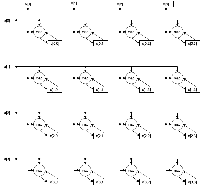
The above array is not suggested for use, as compute exceeds the load bandwidth.
Instead one proposal developed above is
a
multiply/add array with two accumulators per unit for two cycle
accumulation
to
accumulators. This is illustrated below
for :

A
multiply/add array with four accumulators per unit
for
accumulation is illustrated below
for .
Such an array would be used four times over four cycles, each cycle
sourcing from a different combination
of 𝑉
elements from
the
elements loaded from 𝐴 and
the
elements loaded from 𝐵.
This is one possibility explained above for
supporting
or simply to improve performance energy efficiency
for .

For the general case of a tile, the load cycles are and the computation cycles using a array are . Balancing these is not always possible.
The sequence for is illustrated below, using superscripts to indicate cycle numbers, as in to indicate accumulators being zero on cycle 0, the value loaded on cycle 0, the vector loaded on cycle 1, the result of the first half of the two-cycle latency outer product, the result of the second half of the outer product, etc.
The following series of transforms demonstrates how the simple, classic matrix multiply written as three nested loops shown below is transformed to use tiles with an outer product multiply/add/accumulator array. For the tiling, usually TR=TC=V or TR=TC=2V, but there may be implementations that choose other vector lengths for microarchitectural reasons, and this should be supported.
    for i ← 0 to m-1
      for j ← 0 to n-1
	for l ← 0 to k-1
	  c[i,j] ← c[i,j] + a[i,l] * b[l,j]
The above code is then tiled to become the following:
    // iterate over TR×TC tiles of C
    for ti ← 0 to m-1 step TR
      for tj ← 0 to n-1 step TC
	// add product of a[ti..ti+TR-1,0..k-1]
	// and b[0..k-1,tj..tj+TC-1] to tile
	for i ← 0 to TR-1
	  for j ← 0 to TC-1
	    for l ← 0 to k-1
	      c[ti+i,tj+j] ← c[ti+i,tj+j] + a[ti+i,l] * b[l,tj+j]
The above code is modified to use an accumulator tile:
    for ti ← 0 to m-1 step TR
      for tj ← 0 to n-1 step TC
	// copy to accumulator
	for i ← 0 to TR-1
	  for j ← 0 to TC-1
	    acc[i,j] ← c[ti+i,tj+j]
	// add product of a[ti..ti+TR-1,0..k-1]
	// and b[0..k-1,tj..tj+TC-1] to tile
	for i ← 0 to TR-1
	  for j ← 0 to TC-1
	    for l ← 0 to k-1
	      acc[i,j] ← acc[i,j] + a[ti+i,l] * b[l,tj+j]
	// copy accumulator back to tile
	for i ← 0 to TR-1
	  for j ← 0 to TC-1
	    c[ti+i,tj+j] ← acc[i,j]
The above code is then vectorized by moving the l loop
outside and the i and j loops into the
outer product instruction:
    for ti ← 0 to m-1 step TR
      for tj ← 0 to n-1 step TC
	for i ← 0 to TR-1
	  acc[i,0..TC-1] ← c[ti+i,tj..tj+TC-1]	// TC-element vector load + acc write
	for l ← 0 to k-1
	  va ← a[ti..ti+i+TR-1,l]		// TR-element vector load col of A
	  vb ← b[l,tj..tj+i+TC-1]		// TC-element vector load row of B
	  acc ← acc + outerproduct(va, vb)	// 2-cycle outer product instruction
	for i ← 0 to TR-1
	  c[ti+i,tj..tj+TC-1] ← acc[i,0..TC-1]	// acc read + TC-element vector store
where the outerproduct(va, vb) operation invoked above is defined as follows:
	for i ← 0 to TR-1
	  for j ← 0 to TC-1
	    product[i,j] ← va[i] * vb[j]
	return product
In the Matrix Algebra section it was observed that cycle count for matrix multiplication with the smarter variant of unbounded multiply/add units (i.e., units) pipelined to produce a value every cycle takes cycles. It is worth answering how the above method fares relative to this standard applied to a single tile. Because we cut the number of multiply/add units in half to match the load bandwidth, we expect at least twice the cycle count, and this expectation is met: matching a memory system that delivers 𝑉 elements per cycle, a tile of processed by an array of multiply/add units () produces the tile in cycles. It may help to work an example. For a memory system delivering one 512‑bit cache block per cycle and 16‑bit data (e.g., BF16), , and the 32×32 tile is produced using 2 vector loads and one 2‑cycle outer product instruction iterated 32 times taking 64 cycles yielding 512 multiply/adds per cycle. However, this does not include the time to load the accumulators before and transfer them back to 𝐶 after. When this 64 cycle tile computation is part of a 1024×1024 matrix multiply, this tile loop will be called 32 times for each tile of 𝐶. If it takes 64 cycles to load the accumulators from memory and 64 cycles to store back to memory, then this is 64+32×64+64=2176 total cycles. There are a total of 1024 output tiles, so the matrix multiply is 2228224 cycles (not counting cache misses) for 10243 multiply/adds, which works out to 481.88 multiply/adds per cycle, or 94% of peak.
Note that there is no point in loading entire tiles, as this would not benefit performance. Rows and columns are loaded and consumed, and not used again. Storing whole tiles of the 𝐴 and 𝐵 matrixes would only be useful in situation when such a tile is used repeatedly, which does not occur in a larger matrix multiply. This does occur for the accumulation tile of the 𝐶 matrix, which does make that worth storing locally. The question is where it should be stored.
It is worth noting that the l loop above can be unrolled to
create more scheduling opportunities as shown below:
    for ti ← 0 to m-1 step TR
      for tj ← 0 to n-1 step TC
	for i ← 0 to TR-1
	  acc[i,0..TC-1] ← c[ti+i,tj..tj+TC-1]	// TC-element vector load + acc write
	for l ← 0 to k-1 step 4
	  acc ← acc + outerproduct(a[ti..ti+i+TR-1,l+0], b[l+0,tj..tj+i+TC-1])
	  acc ← acc + outerproduct(a[ti..ti+i+TR-1,l+1], b[l+1,tj..tj+i+TC-1])
	  acc ← acc + outerproduct(a[ti..ti+i+TR-1,l+2], b[l+2,tj..tj+i+TC-1])
	  acc ← acc + outerproduct(a[ti..ti+i+TR-1,l+3], b[l+3,tj..tj+i+TC-1])
	for i ← 0 to TR-1
	  c[ti+i,tj..tj+TC-1] ← acc[i,0..TC-1]	// acc read + TC-element vector store
The transpose and packing phase would then arrange the above
non-contiguous vectors to be packed contiguously so that 4×TR and
4×TC element loads would be used. It is also apparent that either
the outerproduct operation should be at least Δ cycles so that
the acc dependency does not stall. It would also be
possible to implement an inner product operation of reduced latency for
the above (e.g., using carry-save arithmetic).
The bandwidth of reads and writes to outer product accumulators far exceeds what a Vector Register File (VRF) generally targets, which suggests that that these structures be kept separate. Also the number of bits in the accumulators is potentially large relative to VRF sizes. Increasing the bandwidth and potentially the size of the VRF to meet the needs of outer product accumulation is not a good solution. Rather the accumulator bits should located in the multiply/add array, and be transferred to memory when a tile is completed. This transfer might be one row at a time through the VRF, since the VRF has the necessary store operations and datapaths to the cache hierarchy. The appropriateness of separate accumulator storage may be illustrated by examples. A typical vector load width might be the cache block size of 512 bits. This represents 64 8‑bit elements. If the products of these 8‑bit elements is accumulated in 16 bits (e.g., int16 for int8 or fp16 for fp8), then for , 16×642 = 65536 bits of accumulator are required. The entire SecureRISC VRF is only twice as many bits, and these bits require more area than accumulator bits, as the VRF must support at least 4 read ports and 2 write ports for parallel execution of vector multiply/acc and a vector load or vector store. In contrast, accumulator storage within the multiply/add array is local, small, and due to locality consumes negligible power. As another example, consider the same 512 bits as sixteen IEEE 754 binary32 elements with . The method for this latency suggests a 16×8 array of binary32 multiply/add units with 2048 32‑bit accumulators, which is again a total of 65536 bits of accumulator storage, but now embedded in much larger multiply/add units.
The number of bits require for accumulation needs to be determined (the example above is not meant to be anything other than an example). Recently the TF32 format appears to be gaining popularity for AI applications, and so accumulation in TF32 for BF16 inputs is one option. However, this needs further investigation.
SecureRISC has instructions that produce
the outer product![]() of two vectors and add this to one of four matrix accumulators. The
matrix accumulators are expected to be stored within the logic producing
the outer product, and so are distinct from the vector register file.
The outer product hardware allows a large number of multiply/accumulate
units to accelerate matrix multiply more efficiently than using vector
operations.
of two vectors and add this to one of four matrix accumulators. The
matrix accumulators are expected to be stored within the logic producing
the outer product, and so are distinct from the vector register file.
The outer product hardware allows a large number of multiply/accumulate
units to accelerate matrix multiply more efficiently than using vector
operations.
The purpose of providing 4 accumulators per multiply/add unit is to allow the accumulators to be loaded and stored by software while outer products are being accumulated to other registers and to allow multiple tiles to be pipelined.
SecureRISC has a large number of registers that affect instruction execution. These registers, called CSRs, are accessed by special instructions that support reading, writing, swapping, setting bits, and clearing bits. Many ISAs have such instructions; the unusual aspect of SecureRISC is first that CSRs are split into early (XCSRs) and late (SCSRs), per-ring registers (RCSRs), ring-enable registers (RECSRs), and indirect CSRs (ICSRs).
RCSRs can be accessed in two ways: first, via the CSR number in the immediate field and ring from an XR; and second via an encoding that refers to the register for the current ring of execution (PC.ring). In addition, RCSRs also have an associated enable CSR, with a 3‑bit ring number specifying which rings may access the register (if it proves useful, an 8‑bit mask could be used). The access test for the x[ring] RCSR is ring ≤ PC.ring & ring ≤ xRE. Only ring 7 may access xRE RECSRs. RECSRs may be read and written individually, or in groups of sixteen, packed into 4‑bit fields of a 64‑bit read or write, which facilitates context switch.
ICSRs are accessed with a CSR base immediate, CSR index from an XR and an offset for the word of data at that index. For example, the ENCRYPTION ICSRs have five 64‑bit values for a given index (an 8‑bit algorithm and 256 bits of encryption key). Similarly the amatch ICSRs have five 64‑bit values for a given index (the address to match, 128 bits of region access permission, and 128 bits of region write permission).
XCSRs, RECSRs, RCSRs, and ICSRs are read and written to and from the XRs. Late pipeline SCSRs are read and written to and from the SRs.
Read and writing CSRs have no side effects. However, reads and writes may affect performance and so it is desirable to provide read-only and write-only versions of CSR operations. However, this introduces five variants, which requires a three-bit instruction field. It may be that CSR operations are changed to always return the old value of the CSR (i.e., always perform a read), which if not useful, wastes a register and perhaps affects performance. This is TBD.
Per-ring CSRs (RCSRs) appear to be fairly expensive, but the invention of SRAM cells in 5 nm and later process nodes that support efficient small RAM means that some RCSRs can by implemented by tiny 8‑entry SRAM arrays, provided that multiple ring values are not required in the same cycle. Unfortunately OoO microarchitectures might produce such a situation, but in some cases this could be handled by reading the necessary RCSRs during instruction decode and pipelining that value along. Other tricks might be used to keep RCSRs as tiny SRAMs.
In the specifications below, the definition of n ← op(o,v,m) comes from the opcode (mnemonic RW for Read-Write, mnemonic RS for Read-Set, mnemonic RC for Read-Clear). Here o is the old value, v is the operand value, and m is the per-CSR bitmask specifying which bits are writeable (some bits possibly being read-only).
| Description | op | Definition | Supported | Reserved |
|---|---|---|---|---|
| Read | R | n ← o | All | |
| Read-Write | RW | n ← (o & ~m) | (v & m) | All | |
| Write | W | |||
| Read-Set | RS | n ← o | (v & m) | XCSRs, RCSRs, ICSRs, SCSRs | RECSRs |
| Read-Clear | RC | n ← o & ~(v & m) | XCSRs, RCSRs, ICSRs, SCSRs | RECSRs |
| Read-Write Group | RW | see below | RECSRs | XCSRs, RCSRs, ICSRs, SCSRs |
Note: the following ignores whether the CSRs in question can store a tag or not. These details will be provided in the future. At the present time, there are no XCSRs, SCSRs, or ICSRs that have tags. This could, however, change in the future. If CHERI is implemented, then tags would be requrired on anything holding an address. Also, at present, no RCSRs have full tags, but CSP and ExcHandler store a ring number in bits 66..64. CSP reads supply 24 as the five high bits on a read, giving the tag the values 192..199. ExcHandler reads supply 26 as the five high bits on a read, giving the tag the values 208..215.
SecureRISC has two sorts of instructions for synchronization via memory
locations. The first is one of the primitives that can implement most
synchronization
methods: Compare And Swap![]() ).
Compare And Swap (CAS) exists for
the SRs
(CASS, CASSD, CASS64, CASS128,
CASSI, CASSDI, CASS64I, CASS128I).
and perhaps the XRs
(CASX, CASXD, CASX64, CASX128,
CASXI, CASXDI, CASX64I, CASX128I)
It is possible that 8, 16, and 32‑bit versions of Compare And Swap
might also be provided. It is also plausible that 288‑bit (half
cache block) and 576‑bit (whole cache block) CAS may be provided
from the VRs.
The basic schema of CAS is illustrated by the
following simplified semantics of CASS64,
with the other instruction formats being similar:
).
Compare And Swap (CAS) exists for
the SRs
(CASS, CASSD, CASS64, CASS128,
CASSI, CASSDI, CASS64I, CASS128I).
and perhaps the XRs
(CASX, CASXD, CASX64, CASX128,
CASXI, CASXDI, CASX64I, CASX128I)
It is possible that 8, 16, and 32‑bit versions of Compare And Swap
might also be provided. It is also plausible that 288‑bit (half
cache block) and 576‑bit (whole cache block) CAS may be provided
from the VRs.
The basic schema of CAS is illustrated by the
following simplified semantics of CASS64,
with the other instruction formats being similar:
ea ← AR[a]
expected ← SR[b]
new ← SR[c]
m ← lvload64(ea)
if m = expected then
lvstore64(ea) ← new
endif
SR[d] ← m
This specification clearly violates the number of read and write ports
for the XRs,
and the CASX forms might be omitted, but
CAS instructions are likely at least two cycle instructions, and might
read the register file over two cycles. However, it is possible that a
CSR could be introduced for the expected value, though this would mean
longer instruction sequences for synchronization. TBD.
The second synchronization is not as powerful as Compare And Swap, and
could be implemented by CAS, but it may be more efficient in some
circumstances. It is atomic load and add
(AADDX64,
and AADDS64).
These instructions load the specified memory location into the
destination register and then atomically increment the memory location,
as illustrated by the following simplified semantics
of AADDX64:
m ← lvload64(ea)
t ← m + 1
lvstore64(ea) ← t
XR[d] ← m
These operations correspond to the ticket(S) operation on a
sequencer, as defined
in Synchronization with Eventcounts and Sequencers![]() by Reed and Kanodia, though sequencers only require an atomic increment,
the generalization to AADDX64 etc. keeps
the system interconnect transaction for uncached atomic add similar to
atomic AND and OR below.
by Reed and Kanodia, though sequencers only require an atomic increment,
the generalization to AADDX64 etc. keeps
the system interconnect transaction for uncached atomic add similar to
atomic AND and OR below.
The third synchronization instructions are even less powerful than
atomic increment, and could be implemented by CAS, but may be more
efficient in some circumstances, such as the GC mark phase for updating
bitmaps. The instructions are atomic
AND (AANDX64), atomic
OR (AORX64), and atomic
XOR (AXORX64). These instructions load
the specified memory location into the destination register and then
atomically AND, OR, or XOR the memory location, as illustrated by the
following simplified semantics
of AANDX64:
m ← lvload64(ea)
t ← m & XR[b]
if t ≠ m then
lvstore64(ea) ← t
endif
XR[d] ← m
The case for RISC‑V’s
AMOSWAP, AMOMIN,
and AMOMAX
seem unclear at this point. (The case for
RISC‑V’s AMOXOR is also
unclear to this author, but it is trivial given support
for AANDX64
and AORX64, and also called for
by C++11 std::atomic![]() and so included.)
Some APIs (e.g., CUDA) may expect these operations, but they could be
implemented on SecureRISC with CAS instructions. C++20 added atomic
operations on floating-point types, but these are best done using CAS
(e.g., it is not appropriate to have floating-point addition in memory
controller for uncached operations).
and so included.)
Some APIs (e.g., CUDA) may expect these operations, but they could be
implemented on SecureRISC with CAS instructions. C++20 added atomic
operations on floating-point types, but these are best done using CAS
(e.g., it is not appropriate to have floating-point addition in memory
controller for uncached operations).
Atomic operations may be performed by the processor on coherent memory locations in the cache by holding off coherency transactions during the operations involved, or on uncached locations by sending a transaction to the memory, which performs the operation atomically there and returns the result. The System Interconnect Address Attributes section describes main memory attributes indicating which locations implement uncached atomic memory operations. The locations to be modified by atomic operations must not cross a 64‑byte boundary; for example, the address for CASS64 must be in the range 0..56 mod 64.
SecureRISC, having committed to providing Compare and Swap (CAS), has not included the Load and Store Conditional paradigm. RISC architectures, have typically begun with this simpler primitive to avoid CAS, and then later added CAS. SecureRISC seeks to avoid this evolution.
SecureRISC will have the usual instructions to wait for an interrupt. Such instructions increase efficiency. While the details are TBD, for example, there might be a WAIT instruction that takes a value to write to IntrEnable[PC.ring], and then suspends fetch before the next instruction (so that the return from the interrupt exception returns to that instruction).
A more interesting instruction under consideration is one that waits for
a memory location to change, which may be useful for reducing the
overhead of memory based synchronization. The
ITS![]() .HANG
UUO and the
x86 MONITOR/MWAIT instructions may be one
model.
.HANG
UUO and the
x86 MONITOR/MWAIT instructions may be one
model.
Note: SecureRISC has acquire and release options for loads and stores, which reduces (but does not eliminate) the need for some memory fences. Fences for virtual memory changes may be necessary, though it may be possible to handle those in the coherence protocol. Some fence instructions may also be useful in mitigating security vulnerabilities due to microarchitecture bugs.
The details of SecureRISC’s fence instructions are TBD, but it is likely to specify a first set of (e.g., as a bitmask) of operations that must complete before a second set (also a bitmask) of operations are allowed initiate. This is similar to what RISC‑V adopted for memory fences (their FENCE instruction, where there are only four set elements), but for a larger set of instructions. The goal is to encompass the variety of fences found in other ISAs. The set elements might include instruction fetch, loads, stores, CSR reads, CSR writes, and other instructions. Loads and stores could be further categorized by System Interconnect Address Attributes or acquire and release attributes. Other operations that might be receive bits in the sets might be related to prediction, system interconnect transactions, error checking, privilege level changes, prefetch, address space changes, waits, interrupts, and exceptions, and so on. One goal is to correctly handle Just-in-Time (JIT) compilation in the presence of processor migration, which should be easier in SecureRISC because stores must invalidate instruction caches. An enlarged set of things to fence should also allow for finer-grain patching of security vulnerability bugs that seem to plague speculative processors; even though these should be handled correctly by processor designers, they seem to often not be handled properly. Not all of this is thought out. Again, the details are TBD.
Note: Need to look at POWER persistent synchronization
instructions (phwsync
and plwsync).
See Power ISA Version 3.1B![]() section 4.6.3 Memory Barrier Instructions.
section 4.6.3 Memory Barrier Instructions.
SecureRISC lacks a System Call instruction (e.g., RISC‑V ECALL), as gates are the preferred method of making requests of higher privilege levels.
SecureRISC has instructions for compiler-directed prefetching and to
control automatic prefetching. These instructions operate on
8‑word cache lines. The C prefix to
these assembler mnemonics represents Cache
. Rather than identify
caches as L1 BBDC, L1 Instruction, L2 Instruction, L1 Data, L2 Data, L3,
etc. we designate caches by referencing the instructions that use those
caches. Further work is required for things that operate on or stop at
some intermediate level of the hierarchy. These instructions operate on
cache block specified by an lvaddr and are subject to access
permissions. They are available to all rings. There will be privileged
instructions not yet listed here.
SecureRISC requires that writes invalidate or update all caches that
contain previous fetches, including the BBDC and L1 and L2 Instruction
caches. Previously fetched instructions still in the pipeline are not
invalidated, so a fence is required. Thus, cache operations are not
required for JIT compilers, merely the fence. This is typically
implemented by having a directory at what ARM calls
the Point of Unification![]() (PoU)
in the cache hierarchy. This directory records the locations in lower
levels which may contain the a copy. Stores consult the directory
and when other locations are noted, those locations are invalidated or
updated.
For multiprocessor systems, a first processor may write instructions that
a second will execute. The first processor must execute a fence to
ensure all writes have completed before signaling the second processor
to proceed. The second processor must also use a fence to ensure that
the pipeline has stale instructions (e.g., fetched speculatively). The
details will be spelled out when the fence instructions are specified.
(PoU)
in the cache hierarchy. This directory records the locations in lower
levels which may contain the a copy. Stores consult the directory
and when other locations are noted, those locations are invalidated or
updated.
For multiprocessor systems, a first processor may write instructions that
a second will execute. The first processor must execute a fence to
ensure all writes have completed before signaling the second processor
to proceed. The second processor must also use a fence to ensure that
the pipeline has stale instructions (e.g., fetched speculatively). The
details will be spelled out when the fence instructions are specified.
Is TLB prefetching required?
| Instruction | Operation |
|---|---|
|
Fetch prefetching and eviction designation (these may be executed too late in the pipeline to be useful an so may be replaced by BBD features) |
|
| CPBB | Prefetch into Basic Block Descriptor Cache (BBDC) |
| CPI | Prefetch into Basic Block Descriptor Cache (BBDC) and Instruction Cache |
| CEBB | Designate eviction candidate for Basic Block Descriptor Cache (BBDC) |
| CEI | Designate eviction candidate for Basic Block Descriptor Cache (BBDC) and Instruction Caches |
| Early pipeline prefetching, zeroing, writeback, invalidation, and eviction designation | |
| CPLA | Prefetch for LA/LAC/etc. |
| CPLX |
Prefetch for LX/etc. (probably identical to CPLA in most cases) |
| CPSA | Prefetch for SA/SAC/etc. |
| CPSX |
Prefetch for SX/etc. (probably identical to CPSA in most cases) |
| CZA | Zero cache block used for SA/SAC/etc. |
| CZX |
Zero cache block used for SX/etc. (probably identical to CZA in most cases) |
| CEA | Designate eviction candidate for LA/SA |
| CEX | Designate eviction candidate for LX/SX |
| CCX | Clean (writeback) for SX cache |
| CCIX | Clean (writeback) and invalidate for SX cache |
|
Late pipeline prefetching, zeroing, writeback, invalidation, and eviction designation (the primary difference from early prefetching is some microarchitectures may not prefetch to the first stage(s) of the data cache hierarchy) |
|
| CPLS | Prefetch for LS |
| CPSS | Prefetch for SS |
| CZS | Zero cache block used for SS/etc. |
| CES | Designate eviction candidate for LS/SS |
| CCS | Clean (writeback) for SS cache |
| CCIS | Clean (writeback) and invalidate for SS cache |
Need to look at POWER dcbstps (data cache block store to persistent storage) and dcbfps (data cache block flush to persistent storage).
The primary issue with fetch prefetching is that some implementations may execute explicit instructions too late to be useful. Eventually I expect to define new next codes in Basic Block Descriptors for L1 BBDC and L1 Instruction Cache prefetch and eviction designation to solve this problem. Whether some of the above instructions are removed by such a solution is TBD.
Prefetch may want additional options for rereference interval prediction and similar hints to avoid removing useful cache blocks when streaming data larger than the cache size.
It is likely appropriate to add some instructions that exist only for code size reduction, which expand into multiple SecureRISC instructions early in the pipeline (e.g., before register renaming). The best candidates for this so far are doubleword load/store instructions, which would expand into two singleword load/store instructions. This expansion and execution as separate instructions in the backend of the pipeline avoids the issues with register renaming that would otherwise exist. The partial execution of part of the pair would be allowed (and loads to the source registers would be not allowed). Doubleword load/store significantly reduce the size of function call entry and exit and may be useful for loading a code pointer and context pointer pair for indirect calls.
The following outlines some of the instructions without giving them their full definitions, which includes tag and bounds checking. The full definitions will follow later.
The 16‑bit instruction formats are included for code density. Some evaluation of whether it is worth the cost should be considered. Note that the BB descriptor gives the sizes of all instructions in the basic block in the form of the start bit mask, and so the instruction size is not encoded in the opcodes. The start mask allows multiple instructions to be decoded in parallel without parsing the instruction stream; in effect it provides an extra bit of information for every 16 bits of the instruction stream.
Because the identical or nearly identical instructions may exist in multiple widths, a convention for distinguishing them is required. Since 32‑bit instructions are most common, these have the shortest form. Mnemonics for instruction sizes other than 32 bits are indicated by their first letter:
| Size | Mnemonic prefix |
|---|---|
| 16 | 1 |
| 32 | |
| 48 | 3 |
| 64 | 4 |
Instructions that calculate an effective address are distinguished by the first letter of their mnemonic: Address, Load, or Store. For loads and stores, the second letter of the mnemonic gives the destination register file either A for ARs, X for XRs, S for SRs, M for VMs, or V for VRs. (There are no loads or stores to the BRs.) The next field of the mnemonic is empty for word loads and stores, or the size (8, 16, 32, or 64—possibly 128?) for sub-word loads and stores to the XRs or SRs. Word stores must be word-aligned, but 64‑bit (possibly 128? sub-word stores may be misaligned and generate an integer tag. Sub-word loads for 8, 16, or 32 bits next include S for signed or U for unsigned. Finally, the last letter is I for an immediate offset (as opposed to a XR[b] offset).
As examples of the above rules: A stores the address calculation AR[a] +p XR[b]<<sa to destination AR[d] while 1AI stores the address calculation AR[a] +p imm8. LA and LAI loads the contents of those two address calculation to the destination AR[d]. LX32U loads XR[d] from an unsigned 32‑bit memory location located using a XR[b] offset and LS16SI loads SR[d] from a signed 16‑bit memory location located using an immediate offset.
Arithmetic instructions use the operation (e.g., ADD or SUB) with a suffix X or S for the register file of the source and destination operands. If an immediate value is one of the operands, a final I is appended. For vector operations the suffixes are VV for vector-vector VS for vector-scalar, and VI for vector-scalar immediate.
As examples of the above rules:
| Assembler | Simplified meaning (ignoring details) |
|---|---|
| ADDXI d, a, imm | XR[d] ← XR[a] + imm |
| ADDS d, a, b | SR[d] ← SR[a] + SR[b] |
For Floating-Point operations, F is used for
IEEE754 binary32 (single-precision), D is
used for IEEE754 binary64
(double-precision), H is used for IEEE754
binary16 (half-precision), B is used for the
non-standard Machine Learning (ML) 16‑bit Brain Float
format,
and P3, P4,
and P5 are used for the three proposed IEEE
binary8pp formats for ML quarter-precision (8‑bit) with
5‑bit, 4‑bit, 3‑bit
exponents. Q is reserved for a future
IEEE754 binary128 (quad-precision).
Some floating-point examples are as follows:
| Assembler | Simplified meaning (ignoring details) | Comment |
|---|---|---|
| FNMADDS d, a, b, c | SR[d] ← −(SR[a] ×f SR[b]) +f SR[c] | |
| DMADDVS d, a, b, c | VR[d] ← (VR[a] ×d SR[b]) +d VR[c] | |
| P4MBSUBVV d, c, a, b | VR[d] ← (VR[a] ×p4b VR[b]) −b VR[c] | P4 widening to BF multiply-subtract |
| Mnemonic | Definition | Comment | Exp | Prec |
|---|---|---|---|---|
| Q |
binary128 |
quadruple-precision | 15 | 113 |
| D |
binary64 |
double-precision | 11 | 53 |
| F |
binary32 |
single-precision | 8 | 24 |
| H |
binary16 |
half-precision | 5 | 11 |
| B |
bfloat16 |
ML alternative to half-precision | 8 | 8 |
| P5 | binary8p5 |
quarter-precision for ML alternative | 3 | 5 |
| P4 | binary8p4 |
quarter-precision for ML alternative | 4 | 4 |
| P3 | binary8p3 |
quarter-precision for ML | 5 | 3 |
SecureRISC has not yet considered inclusion
of NVIDIA’s Tensor Float format![]() .
.
In the following sections, sometimes a set of instructions are defined with a mnemonic schema using the following:
| What | Schema | Mnemonic | Definition | Comment |
|---|---|---|---|---|
| Operation Mnemonic schemas for ARs | ||||
| Address Comparison |
ac | EQ | x63..0 = y63..0 | |
| NE | x63..0 ≠ y63..0 | |||
| LTU | x63..0 <u y63..0 | |||
| GEU | x63..0 ≥u y63..0 | |||
| TEQ | x71..64 = y7..0 | tag equal | ||
| TNE | x71..64 ≠ y7..0 | tag not-equal | ||
| TLTU | x71..64 <u y7..0 | tag less than | ||
| TGEU | x71..64 ≥u y7..0 | tag greater than or equal | ||
| WEQ | x71..0 = y71..0 | word equal | ||
| WNE | x71..0 ≠ y71..0 | word not-equal | ||
| WLTU | x71..0 <u y71..0 | word less than | ||
| WGEU | x71..0 ≥u y71..0 | word greater than or equal | ||
| Operation Mnemonic schemas for XRs | ||||
| Index Arithmetic |
xa | ADD | x63..0 + y63..0 | mod 264 addition |
| SUB | x63..0 − y63..0 | mod 264 subtraction | ||
| MINU | minu(x63..0, y63..0) | |||
| MINS | mins(x63..0, y63..0) | |||
| MINUS | minus(x63..0, y63..0) | |||
| MAXU | maxu(x63..0, y63..0) | |||
| MAXS | maxs(x63..0, y63..0) | |||
| MAXUS | maxus(x63..0, y63..0) | |||
| Index Logical | xl | AND | x63..0 & y63..0 | |
| OR | x63..0 | y63..0 | |||
| XOR | x63..0 ^ y63..0 | |||
| SLL | x63..0 <<u y5..0 | |||
| SRL | x63..0 >>u y5..0 | |||
| SRA | x63..0 >>s y5..0 | |||
| Index Comparison |
xc | EQ | x63..0 = y63..0 | |
| NE | x63..0 ≠ y63..0 | |||
| LTU | x63..0 <u y63..0 | |||
| LT | x63..0 <s y63..0 | |||
| GEU | x63..0 ≥u y63..0 | |||
| GE | x63..0 ≥s y63..0 | |||
| NONE | (x63..0&y63..0)=0 | Check statistics | ||
| ANY | (x63..0&y63..0)≠0 | Check statistics | ||
| ALL | (x63..0&~y63..0)=0 | Check statistics | ||
| NALL | (x63..0&~y63..0)≠0 | Check statistics | ||
| BITC | xy5..0=0 | Check statistics | ||
| BITS | xy5..0≠0 | Check statistics | ||
| TEQ | x71..64 = y7..0 | tag equal | ||
| TNE | x71..64 ≠ y7..0 | tag not-equal | ||
| TLTU | x71..64 <u y7..0 | tag less than | ||
| TGEU | x71..64 ≥u y7..0 | tag greater than or equal | ||
| WEQ | x71..0 = y71..0 | word equal | ||
| WNE | x71..0 ≠ y71..0 | word not-equal | ||
| WLTU | x71..0 <u y71..0 | word less than | ||
| WGEU | x71..0 ≥u y71..0 | word greater than or equal | ||
| Operation Mnemonic schemas for SRs, BRs, VRs, and VMs | ||||
| Boolean | bo | AND | x & y | |
| ANDTC | x & ~y | |||
| NAND | ~(x & y) | |||
| NOR | ~(x | y) | |||
| OR | x | y | |||
| ORTC | x | ~y | |||
| XOR | x ^ y | |||
| EQV | x ^ ~y | |||
| Boolean accumulation |
ba | AND | x & y | |
| OR | x | y | OR with b0 used by assembler for non-accumulation | ||
| Integer Comparison |
ic | EQ | x63..0 = y63..0 | |
| NE | x63..0 ≠ y63..0 | |||
| LTU | x63..0 <u y63..0 | |||
| LT | x63..0 <s y63..0 | |||
| GEU | x63..0 ≥u y63..0 | |||
| GE | x63..0 ≥s y63..0 | |||
| NONE | (x63..0&y63..0)=0 | Check statistics | ||
| ANY | (x63..0&y63..0)≠0 | Check statistics | ||
| ALL | (x63..0&~y63..0)=0 | Check statistics | ||
| NALL | (x63..0&~y63..0)≠0 | Check statistics | ||
| BITC | xy5..0=0 | Check statistics | ||
| BITS | xy5..0≠0 | Check statistics | ||
| Integer Arithmetic |
io | ADD | x63..0 + y63..0 | mod 264 addition |
| SUB | x63..0 − y63..0 | mod 264 subtraction | ||
| ADDOU | x63..0 +u y63..0 | Trap on unsigned overflow | ||
| ADDOS | x63..0 +s y63..0 | Trap on signed overflow | ||
| ADDOUS | x63..0 +us y63..0 | Trap on unsigned-signed overflow | ||
| SUBOU | x63..0 −u y63..0 | Trap on unsigned overflow | ||
| SUBOS | x63..0 −s y63..0 | Trap on signed overflow | ||
| SUBOUS | x63..0 −us y63..0 | Trap on unsigned-signed overflow | ||
| MINU | minu(x63..0, y63..0) | |||
| MINS | mins(x63..0, y63..0) | |||
| MINUS | minus(x63..0, y63..0) | |||
| MAXU | maxu(x63..0, y63..0) | |||
| MAXS | maxs(x63..0, y63..0) | |||
| MAXUS | maxus(x63..0, y63..0) | |||
| MUL | x63..0 × y63..0 | least-significant 64 bits of product | ||
| MULOU | x63..0 ×u y63..0 | Trap on unsigned overflow | ||
| MULOS | x63..0 ×s y63..0 | Trap on signed overflow | ||
| MULUS | x63..0 ×us y63..0 | Trap on unsigned-signed overflow | ||
|
Integer 1-operand (should these be logical accumulations instead?) |
a1 | NEG | − x63..0 | negate |
| ABS | abs(x63..0) | absolute value | ||
| POPC | popcount(x63..0) | count number of one bits | ||
| COUNTS | countsign(x63..0) | count most-significant bits equal to sign bit | ||
| COUNTMS0 | countms0(x63..0) | |||
| COUNTMS1 | countms1(x63..0) | |||
| COUNTLS0 | countls0(x63..0) | |||
| COUNTLS1 | countls1(x63..0) | |||
| Integer Arithmetic accumulation |
ia | ADD | x63..0 + y63..0 | |
| SUB | x63..0 − y63..0 | |||
| y63..0 |
Non-accumulation Mnemonic omitted in assembler: e.g., just ADDS d, a, b is encoded with this ia to perform SR[d] ← SR[a] + SR[b] |
|||
| Bitwise Logical | lo | AND | x63..0 & y63..0 | |
| ANDTC | x63..0 & ~y63..0 | |||
| NAND | ~(x63..0 & y63..0) | |||
| NOR | ~(x63..0 | y63..0) | |||
| OR | x63..0 | y63..0 | |||
| ORTC | x63..0 | ~y63..0 | |||
| XOR | x63..0 ^ y63..0 | |||
| EQV | x63..0 ^ ~y63..0 | |||
| SLL | x63..0 <<u y5..0 | |||
| SRL | x63..0 >>u y5..0 | |||
| SRA | x63..0 >>s y5..0 | |||
| CLMUL | x63..0 ⊗ y63..0 | Carryless multiplication | ||
| Bitwise Logical accumulation |
la | AND | x63..0 & y63..0 | |
| OR | x63..0 | y63..0 | |||
| XOR | x63..0 ^ y63..0 | Primarily for CLMUL | ||
| y63..0 |
Non-accumulation Mnemonic omitted in assembler: e.g., just ANDS d, [c,] a, b is encoded with this la to perform SR[d] ← SR[a] & SR[b] with SR[c] ignored. |
|||
| Floating-Point Arithmetic |
fo | ADD | x +fmt y | |
| SUB | x −fmt y | |||
| MIN | minfmt(x, y) | |||
| MAX | maxfmt(x, y) | |||
| MINM | minmagfmt(x, y) | |||
| MAXM | maxmagfmt(x, y) | |||
| M | x ×fmt y | |||
| NM | −(x ×fmt y) | negative multiply | ||
| Mw | w(x) ×w w(y) | widening multiply | ||
| NMw | −(w(x) ×w w(y)) | widening negative multiply | ||
| DIV | x63..0 ÷fmt y63..0 | Must be no-accumulation | ||
| Floating-Point accumulation |
fa | ADD | x +fmt y | |
| SUB | x −fmt y | |||
| y63..0 |
Non-accumulation Mnemonic omitted in assembler: e.g., just DADDS d, a, b is encoded with this fa to perform SR[d] ← SR[a] +d SR[b] |
|||
| Floating-Point 1-operand |
f1 | MOV | x | |
| NEG | −fmt x63..0 | |||
| ABS | absfmt(x63..0) | |||
| RECIP | 1.0 ÷fmt x63..0 | |||
| SQRT | sqrtfmt(x63..0) | |||
| RSQRT | rsqrtfmt(x63..0) | |||
| FLOOR | floorfmt(x63..0) | |||
| CEIL | ceilfmt(x63..0) | |||
| TRUNC | truncfmt(x63..0) | |||
| ROUND | roundfmt(x63..0) | |||
| CVTI | converti,fmt(x63..0) | |||
| CVTB | convertb,fmt(x63..0) | |||
| CVTH | converth,fmt(x63..0) | |||
| CVTF | convertf,fmt(x63..0) | |||
| CVTD | convertd,fmt(x63..0) | |||
| FLOATU | floatfmt,u(x63..0, imm) | |||
| FLOATS | floatfmt,s(x63..0, imm) | |||
| CLASS | classfmt(x63..0) | |||
| Floating-Point Comparison |
fc | OR | x63..0 ?fmt y63..0 | ordered |
| UN | x63..0 ~?fmt y63..0 | unordered | ||
| EQ | x63..0 =fmt y63..0 | |||
| NE | x63..0 ≠fmt y63..0 | |||
| LT | x63..0 <fmt y63..0 | |||
| GE | x63..0 ≥fmt y63..0 | |||
| LE | x63..0 ≤fmt y63..0 | |||
| GT | x63..0 >fmt y63..0 | |||
| Class | Schema | Definition | Examples |
|---|---|---|---|
| Integer Arithmetic | ioia | SR[d] ← SR[c] ia (SR[a] io SR[b]) | MADDS |
| Bitwise Logical | lola | SR[d] ← SR[c] la (SR[a] lo SR[b]) | ANDORS |
| Floating-Point | fofa | SR[d] ← SR[c] fafmt (SR[a] fofmt SR[b]) | DNMSUBS |
| Boolean | boba | BR[d] ← BR[c] ba (BR[a] bo BR[b]) | ANDORS |
| VM[d] ← VM[c] ba (VM[a] bo VM[b]) | ORANDM | ||
| Integer Comparison | icba | BR[d] ← BR[c] ba (SR[a] ic SR[b]) | LTUANDS |
| Floating-Point Comparison | fcba | BR[d] ← BR[c] ba (SR[a] fc SR[b]) | DLTANDS |
| Value | Mnemonic | Function | Mnemonic | Function |
|---|---|---|---|---|
| 0000 | F | 0 | ||
| 0001 | NOR | a ~| b | ANDCC | ~a & ~b |
| 0010 | ANDTC | a & ~b | ||
| 0011 | NOTB | ~b | ||
| 0100 | ANDCT | ~a & b | ||
| 0101 | NOTA | ~a | ||
| 0110 | XOR | a ^ b | ||
| 0111 | NAND | a ~& b | ORCC | ~a | ~b |
| 1000 | AND | a & b | ||
| 1001 | EQV | a ~^ b | XNOR | ~(a ^ b) |
| 1010 | A | a | ||
| 1011 | ORTC | a | ~b | ||
| 1100 | B | b | ||
| 1101 | ORCT | ~a | b | ||
| 1110 | OR | a | b | ||
| 1111 | T | 1 |
| m | What | Example mnemonic |
|---|---|---|
| 0 | Reserved | |
| 1 | Unsigned | MINU |
| 2 | Signed | MAXS |
| 3 | Unsigned Signed | MINUS |
| m | What | Example mnemonic |
|---|---|---|
| 0 | wrap | ADD |
| 1 | Overflow Unsigned | SUBOU |
| 2 | Overflow Signed | MULOS |
| 3 | Overflow Unsigned Signed | ADDOUS |
| field TBD |
Static | Dynamic |
|---|---|---|
| 0 | Nearest, ties to Even | |
| 1 | Round to odd |
|
| 2 | Nearest, ties to Min Magnitude | |
| 3 | Nearest, ties to Max Magnitude | |
| 4 | Toward −∞ (floor) | |
| 5 | Toward +∞ (ceiling) | |
| 6 | Toward 0 (truncate) | |
| 7 | Dynamic | Away from 0 |
| field TBD | Data width |
Aligned | MemTag check |
Examples |
|---|---|---|---|---|
| 0 | 8 | 240..245 | LX8U, LS8SI | |
| 1 | 16 | 240..245 | LS16S, LS16UI | |
| 2 | 32 | 240..245 | SX32I, SS32 | |
| 3 | 64 | 240..252 | LX64UI, SS64 | |
| 4 | 72 | word | LAI, LX, LS, SSI | |
| 5 | 144 | doubleword | LAD, SADI | |
| 6 | 144 | doubleword | 232/251 | LAC, SAC |
| 7 | 64 | clique | CLA64, CSA64 |
| field TBD | Mnemonic | Semantics |
|---|---|---|
| 0 | Neither acquire nor release | |
| 1 | .a | Acquire |
| 2 | .r | Release |
| 3 | .ar | Acquire and Release |
The table below lists the indexed load/store opcode mnemonics, but the
same encoding is used for the immediate offset opcodes (i.e., with the
appended I suffix). The {L,S}{X,S}128
instructions marked with a ?
are possible placeholders for future
code density instructions that expand into a pair of load or store
instructions, similar to the existing {L,S}{X,S}D instructions.
| field TBD |
Reg file |
Operation | field TBD | |||||||
|---|---|---|---|---|---|---|---|---|---|---|
| 0 | 1 | 2 | 3 | 4 | 5 | 6 | 7 | |||
| 0 | XR | Load Unsigned | LX8U | LX16U | LX32U | LX64U | LX | LXD | LX128? | |
| 1 | SR | Load Unsigned | LS8U | LS16U | LS32U | LS64U | LS | LSD | LS128? | |
| 2 | XR | Speculative Load Unsigned | SLX8U | SLX16U | SLX32U | SLX64U | SLX | SLXD | ||
| 3 | SR | Speculative Load Unsigned | SLS8U | SLS16U | SLS32U | SLS64U | SLS | SLSD | ||
| 4 | XR | Load Signed | LX8S | LX16S | LX32S | LX64S | ||||
| 5 | SR | Load Signed | LS8S | LS16S | LS32S | LS64S | ||||
| 6 | XR | Speculative Load Signed | SLX8S | SLX16S | SLX32S | SLX64S | ||||
| 7 | SR | Speculative Load Signed | SLS8S | SLS16S | SLS32S | SLS64S | ||||
| 8 | AR | Load | RLA32 | RLA64 | LA | LAD | LAC | CLA64 | ||
| 9 | VM | Load | LM | |||||||
| 10 | AR | Speculative Load | SRLA32 | SRLA64 | SLA | SLAD | SLAC | SCLA64 | ||
| 11 | Reserved | |||||||||
| 12 | XR | Store | SX8 | SX16 | SX32 | SX64 | SX | SXD | SX128? | |
| 13 | SR | Store | SS8 | SS16 | SS32 | SS64 | SS | SSD | SS128? | |
| 14 | AR | Store | RSA32 | RSA64 | SA | SAD | SAC | CSA64 | ||
| 15 | VM | Store | SM | |||||||
| n | Suffix | What | Example | m usage | f usage |
|---|---|---|---|---|---|
| 0 | S | Scalar integer |
SR[d] ← SR[c] ia (SR[a] io SR[b]) | su or osu | |
| B | Boolean | BR[d] ← BR[c] ba (BR[a] bo BR[b]) | |||
| S | Scalar floating |
SR[d] ← SR[c] fafmt (SR[a] fofmt SR[b]) | round | ||
| 1 | SV | Vector reduction to scalar integer |
SR[d] ← reduction(SR[a], VR[b]) masked by VM[m] and n |
vector mask | |
| SV | Vector reduction to scalar floating |
SR[d] ← reductionfmt(SR[a], VR[b]) masked by VM[m] and n |
vector mask | round | |
| M | Mask | VM[d] ← VM[c] ba (VM[a] bo VM[b]) | |||
| 2 | VS | Vector Scalar integer |
VR[d] ← VR[c] ia (VR[a] io SR[b]) masked by VM[m] and n |
vector mask |
|
| VS | Vector Scalar floating |
VR[d] ← VR[c] fafmt (VR[a] fofmt SR[b]) masked by VM[m] and n |
vector mask |
round | |
| VI | Vector Immediate integer |
VR[d] ← VR[a] io imm masked by VM[m] and n |
vector mask |
||
| VS | Vector Scalar integer compare |
VM[d] ← VM[c] ba (VR[a] ic SR[b]) masked by VM[m] and n |
|||
| VI | Vector Immediate integer compare |
VM[d] ← VR[a] ic imm masked by VM[m] and n |
|||
| VS | Vector Scalar floating compare |
VM[d] ← VM[c] ba (VR[a] fcfmt SR[b]) masked by VM[m] and n |
|||
| 3 | VV | Vector Vector integer |
VR[d] ← VR[c] ia (VR[a] io VR[b]) masked by VM[m] and n |
vector mask |
|
| VV | Vector Vector floating |
VR[d] ← VR[c] fafmt (VR[a] fofmt VR[b]) masked by VM[m] and n |
vector mask |
round | |
| VV | Vector Vector integer compare |
VM[d] ← VM[c] ba (VR[a] ic VR[b]) masked by VM[m] and n |
|||
| VV | Vector Vector floating compare |
VM[d] ← VM[c] ba (VR[a] fcfmt VR[b]) masked by VM[m] and n |
Vector operations write only the destination elements enabled by the vector mask operand. Destination element i is written if VM[m]i = n. Since VM[0] is hardwired to 0, setting m to 0 and n to 0 writes unconditionally. The combination of m = 0 and n = 1 is reserved.
The following are a sketch of the 16‑bit instruction encodings, but the actual encodings will be determined by analyzing instruction frequency in the 32‑bit instruction set.
|
1:0 3:2 |
0 | 1 | 2 | 3 |
|---|---|---|---|---|
| 0 | 1A | 1LA | 1SA | i16da |
| 1 | 1AI | 1LAI | 1SAI | i16ab0 |
| 2 | 1ADDX | 1LX | 1SX | 1XI |
| 3 | 1ADDXI | 1LXI | 1SXI | i16ab1 |
| 15 | 12 | 11 | 8 | 7 | 4 | 3 | 0 | ||||
| b | a | d | op16 | ||||||||
| 4 | 4 | 4 | 4 | ||||||||
| Word address calculation with indexed addressing: 1A | ||
| 1A | d, a, b |
v ← AV[a] & XV[b] trap if v & boundscheck(AR[a], XR[b]<<3) = 0 AR[d] ← AR[a] +p XR[b]<<3 AV[d] ← v |
| Index register addition | ||
| 1ADDX | d, a, b |
XR[d] ← XR[a] + XR[b] XV[d] ← XV[a] & XV[b] |
|
Non-speculative tagged word loads with indexed addressing: L{A,X,S} (LS in 32‑bit table) |
||
| 1LA | d, a, b |
v ← AV[a] & XV[b] trap if v & boundscheck(AR[a], XR[b]<<3) = 0 AR[d] ← v ? lvload72(AR[a] +p XR[b]<<3) : 0 AV[d] ← v |
| 1LX | d, a, b |
v ← AV[a] & XV[b] trap if v & boundscheck(AR[a], XR[b]<<3) = 0 XR[d] ← v ? lvload72(AR[a] +p XR[b]<<3) : 0 XV[d] ← v |
| 15 | 12 | 11 | 8 | 7 | 4 | 3 | 0 | ||||
| imm4 | a | d | op16 | ||||||||
| 4 | 4 | 4 | 4 | ||||||||
| Word address calculation with immediate addressing: AI | ||
| 1AI | d, a, imm4 |
v ← AV[a] trap if v & boundscheck(AR[a], imm4<<3) = 0 AR[d] ← AR[a] +p imm4<<3 AV[d] ← v |
| Index register addition immediate | ||
| 1ADDXI | d, a, imm4 |
XR[d] ← XR[a] + imm4 XV[d] ← XV[a] |
|
Non-speculative tagged word loads with indexed addressing: L{A,X,S}I (LSI and wider immediate LA and LX in 32‑bit table) |
||
| 1LAI | d, a, imm4 |
v ← AV[a] trap if v & boundscheck(AR[a], imm4<<3) = 0 AR[d] ← v ? lvload72(AR[a] +p imm4<<3) : 0 AV[d] ← v |
| 1LXI | d, a, imm4 |
v ← AV[a] trap if v & boundscheck(AR[a], imm4<<3) = 0 XR[d] ← v ? lvload72(AR[a] +p imm4<<3) : 0 XV[d] ← v |
|
13:12 15:14 |
0 | 1 | 2 | 3 |
|---|---|---|---|---|
| 0 | 1NEGX | 1NOTX | 1MOVSX | 1MOVXS |
| 1 | 1RTAGX | 1RTAGA | 1RSIZEA | |
| 2 | 1MOVAX | 1MOVXA | 1MOVAS | 1MOVSA |
| 3 | 1SOBX | 1RTAGS |
| 15 | 12 | 11 | 8 | 7 | 4 | 3 | 0 | ||||
| op16da | a | d | i16da | ||||||||
| 4 | 4 | 4 | 4 | ||||||||
| 1NEGX | d, a |
XR[d] ← −XR[a] XV[d] ← XV[a] |
| 1NOTX | d, a |
XR[d] ← ~XR[a] XV[d] ← AV[a] |
| 1MOVA | d, a |
AR[d] ← AR[a] AV[d] ← AV[a] |
| 1MOVX | d, a |
XR[d] ← XR[a] XV[d] ← XV[a] |
| 1MOVS | d, a |
SR[d] ← SR[a] SV[d] ← SV[a] |
| 1MOVAX | d, a |
AR[d] ← XR[a] AV[d] ← XV[a] |
| 1MOVXA | d, a |
XR[d] ← AR[a] XV[d] ← AV[a] |
| 1MOVSX | d, a |
SR[d] ← XR[a] SV[d] ← XV[a] |
| 1MOVXS | d, a |
XR[d] ← SR[a] XV[d] ← SV[a] |
| 1MOVAS | d, a |
AR[d] ← SR[a] AV[d] ← SV[a] |
| 1MOVSA | d, a |
SR[d] ← AR[a] SV[d] ← AV[a] |
| 1RTAGA | d, a |
XR[d] ← 240 ∥ 056 ∥ AR[a]71..64 XV[d] ← XV[a] |
| 1RTAGX | d, a |
XR[d] ← 240 ∥ 056 ∥ XR[a]71..64 XV[d] ← XV[a] |
| 1RTAGS | d, a |
SR[d] ← 240 ∥ 056 ∥ SR[a]71..64 SV[d] ← SV[a] |
| 1RSIZEA | d, a |
XR[d] ← 240 ∥ 03 ∥ AR[a]132..72 XV[d] ← XV[a] |
| 1SOBX |
trap if XV[a] = 0 XR[d] ← XR[a] − 1 XV[d] ← 1 loop back if XR[d] ≠ 0 |
1NEGX is identical to RSUBXI with an immediate of 0 but is 16 bits rather than 32. Whether this is important is unclear. 1NOTX is identical to RSUBXI with an immediate of -1 but is 16 bits rather than 32. Whether this is important is unclear. Whether to include these will depend on code size statistics.
|
5:3 7:6 |
0 | 1 | 2 | 3 |
|---|---|---|---|---|
| 0 | 1BEQA | 1BNEA | 1BLTAU | 1BGEAU |
| 1 | 1BEQX | 1BNEX | 1BLTXU | 1BGEXU |
| 2 | 1BNONEX | 1BANYX | 1BLTX | 1BGEX |
| 3 | i16a0 |
|
5:4 7:6 |
0 | 1 | 2 | 3 |
|---|---|---|---|---|
| 0 | 1TEQA | 1TNEA | 1TLTAU | 1TGEAU |
| 1 | 1TEQX | 1TNEX | 1TLTXU | 1TGEXU |
| 2 | 1TNONEX | 1TANYX | 1TLTX | 1TGEX |
| 3 | i16a1 |
| 15 | 12 | 11 | 8 | 7 | 4 | 3 | 0 | ||||
| b | a | op16ab | i16ab | ||||||||
| 4 | 4 | 4 | 4 | ||||||||
All of the following first do either
trap if AV[a] & AV[b] = 0
or
trap if XV[a] & XV[b] = 0
as appropriate.
| 1BEQA | a, b | branch if AR[a] = AR[b] |
| 1BEQX | a, b | branch if XR[a] = XR[b] |
| 1BNEA | a, b | branch if AR[a] ≠ AR[b] |
| 1BNEX | a, b | branch if XR[a] ≠ XR[b] |
| 1BLTAU | a, b | branch if AR[a] <u AR[b] |
| 1BLTXU | a, b | branch if XR[a] <u XR[b] |
| 1BGEAU | a, b | branch if AR[a] ≥u AR[b] |
| 1BGEXU | a, b | branch if XR[a] ≥u XR[b] |
| 1BLTX | a, b | branch if XR[a] <s XR[b] |
| 1BGEX | a, b | branch if XR[a] ≥s XR[b] |
| 1BNONEX | a, b | branch if (XR[a] & XR[b]) = 0 |
| 1BANYX | a, b | branch if (XR[a] & XR[b]) ≠ 0 |
| 1TEQA | a, b | trap if AR[a] = AR[b] |
| 1TEQX | a, b | trap if XR[a] = XR[b] |
| 1TNEA | a, b | trap if AR[a] ≠ AR[b] |
| 1TNEX | a, b | trap if XR[a] ≠ XR[b] |
| 1TLTAU | a, b | trap if AR[a] <u AR[b] |
| 1TLTXU | a, b | trap if XR[a] <u XR[b] |
| 1TGEAU | a, b | trap if AR[a] ≥u AR[b] |
| 1TGEXU | a, b | trap if XR[a] ≥u XR[b] |
| 1TLTX | a, b | trap if XR[a] <s XR[b] |
| 1TGEX | a, b | trap if XR[a] ≥s XR[b] |
| 1TNONEX | a, b | trap if (XR[a] & XR[b]) = 0 |
| 1TANYX | a, b | trap if (XR[a] & XR[b]) ≠ 0 |
|
13:12 15:14 |
0 | 1 | 2 | 3 |
|---|---|---|---|---|
| 0 | 1BEQNA | 1BNENA | 1BF | 1BT |
| 1 | 1BEQZX | 1BNEZX | 1BLTZX | 1BGEZX |
| 2 | 1JMPA | |||
| 3 | 1SWITCHX | 1BLEZX | 1BGTZX |
|
13:12 15:14 |
0 | 1 | 2 | 3 |
|---|---|---|---|---|
| 0 | 1TEQNA | 1TNENA | 1TF | 1TT |
| 1 | 1TEQZX | 1TNEZX | 1TLTZX | 1TGEZX |
| 2 | 1CHKVA | 1CHKVX | 1CHKVS | |
| 3 | 1TLEZX | 1TGTZX |
| 15 | 12 | 11 | 8 | 7 | 4 | 3 | 0 | ||||
| op16a | a | i16a | i16ab | ||||||||
| 4 | 4 | 4 | 4 | ||||||||
All of the following first do either
trap if AV[a] = 0
or
trap if XV[a] = 0
or
trap if BV[a] = 0
as appropriate.
| 1BEQNA | a | branch if AR[a]63..0 = 0 |
| 1BNENA | a | branch if AR[a]63..0 ≠ 0 |
| 1BEQZX | a | branch if XR[a]63..0 = 0 |
| 1BNEZX | a | branch if XR[a]63..0 ≠ 0 |
| 1BLTZX | a | branch if XR[a]63..0 <s 0 |
| 1BGEZX | a | branch if XR[a]63..0 ≥s 0 |
| 1BLEZX | a | branch if XR[a]63..0 ≤s 0 |
| 1BGTZX | a | branch if XR[a]63..0 >s 0 |
| 1BF | a | branch if BR[a] = 0 |
| 1BT | a | branch if BR[a] ≠ 0 |
| 1TEQZX | a | trap if XR[a]63..0 = 0 |
| 1TNEZX | a | trap if XR[a]63..0 ≠ 0 |
| 1TLTZX | a | trap if XR[a]63..0 <s 0 |
| 1TGEZX | a | trap if XR[a]63..0 ≥s 0 |
| 1TLEZX | a | trap if XR[a]63..0 ≤s 0 |
| 1TGTZX | a | trap if XR[a]63..0 >s 0 |
| 1TF | a | trap if BR[a] = 0 |
| 1TT | a | trap if BR[a] ≠ 0 |
| 1JMPA | a |
trap if AR[a]71..68 ≠ 12 trap if AR[a]2..0 ≠ 0 trap if PC66..64 ≠ AR[a]66..64 PC ← AR[a]66..0 |
| 1SWITCHX | a |
trap if XR[a]71..65 ≠ 120 PC ← PC +p (XR[a]<<3) |
| 1CHKVA | a | trap if AV[a] = 0 |
| 1CHKVX | a | trap if XV[a] = 0 |
| 1CHKVS | a | trap if SV[a] = 0 |
| 15 | 8 | 7 | 4 | 3 | 0 | |||
| imm8 | d | op16 | ||||||
| 8 | 4 | 4 | ||||||
| 1XI | d, imm8 |
XR[d] ← 240 ∥ imm8748 ∥ imm8 XV[d] ← 1 |
|
1:0 3:2 |
0 | 1 | 2 | 3 |
|---|---|---|---|---|
| 0 | AXload | AXstore | SVload | SVstore |
| 1 | ||||
| 2 | ARop | XRop | SRop | VRop |
| 3 | XI | XUI | SI | SUI |
| 31 | 28 | 27 | 24 | 23 | 22 | 21 | 20 | 19 | 16 | 15 | 12 | 11 | 8 | 7 | 4 | 3 | 0 | |||||||
| op32g | f | n | m | c | b | a | d | op32 | ||||||||||||||||
| 4 | 4 | 2 | 2 | 4 | 4 | 4 | 4 | 4 | ||||||||||||||||
| Scalar Integer | ||
| ioiaS | d, c, a, b |
SR[d] ← SR[c] ia (SR[a] io SR[b]) SV[d] ← SV[a] & SV[b] & SV[c] |
| lolaS | d, c, a, b |
SR[d] ← SR[c] la (SR[a] lo SR[b]) SV[d] ← SV[a] & SV[b] & SV[c] |
| SELS | d, c, a, b |
SR[d] ← BR[c] ? SR[a] : SR[b] SV[d] ← BV[c] & (BR[c] ? SV[a] : SV[b]) |
| BITSELS | d, c, a, b |
SR[d] ← (SR[c] & SR[a]) | (~SR[c] & SR[b]) SV[d] ← SV[a] & SV[b] & SV[c] |
| i1S | d, a |
SR[d] ← i1(SR[a]) SV[d] ← SV[a] |
| Scalar Integer Multiword | ||
| FUNS | d, b, a, c |
t ← (SR[b]63..0∥SR[a]63..0) >> SR[c]5..0 SR[d] ← 240 ∥ t63..0 SV[d] ← SV[a] & SV[b] & SV[c] |
| ROTRS | d, a, b | assembler expands to FUNS d, a, a, b |
| FUNNS | d, b, a, c |
t ← (SR[b]63..0∥SR[a]63..0) >> (−SR[c])5..0 SR[d] ← 240 ∥ t63..0 SV[d] ← SV[a] & SV[b] & SV[c] |
| ROTLS | d, a, b | assembler expands to FUNNS d, a, a, b |
| ADDC | d, b, a |
trap if (SV[a] & SV[b]) = 0 t ← SR[a]63..0 + SR[b]63..0 + CARRY0 CARRY ← 063 ∥ t64 SR[d] ← 240 ∥ t63..0 SV[d] ← 1 |
| MULC | d, b, a, c |
trap if (SV[a] & SV[b] & SV[c]) = 0 t ← (SR[a]63..0 ×u SR[b]63..0) + SR[c]63..0 + CARRY CARRY ← t127..64 SR[d] ← 240 ∥ t63..0 SV[d] ← 1 |
| DIVC | d, b, a, c |
trap if (SV[a] & SV[b]) = 0 q,r ← (CARRY∥SR[a]63..0) ÷u SR[b]63..0 CARRY ← r SR[d] ← 240 ∥ q SV[d] ← 1 |
| Boolean | ||
| boba | d, c, a, b |
BR[d] ← BR[c] ba (BR[a] bo BR[b]) BV[d] ← BV[a] & BV[b] & BV[c] |
| bobaM | d, c, a, b | VR[d] ← VM[c] ba (VM[a] bo VM[b]) |
| Integer Comparison | ||
| acbaA | d, c, a, b |
BR[d] ← BR[c] ba (AR[a] ac AR[b]) BV[d] ← AV[a] & AV[b] & BV[c] |
| xcbaX | d, c, a, b |
BR[d] ← BR[c] xa (XR[a] xc XR[b]) BV[d] ← XV[a] & XV[b] & BV[c] |
| icbaS | d, c, a, b |
BR[d] ← BR[c] ba (SR[a] ic SR[b]) BV[d] ← SV[a] & SV[b] & BV[c] |
| Floating-Point | ||
| Df1S | d, a |
SR[d] ← f1d(SR[a]) SV[d] ← SV[a] |
| Ff1S | d, a |
SR[d] ← f1f(SR[a]) SV[d] ← SV[a] |
| Hf1S | d, a |
SR[d] ← f1h(SR[a]) SV[d] ← SV[a] |
| Bf1S | d, a |
SR[d] ← f1b(SR[a]) SV[d] ← SV[a] |
| P4f1S | d, a |
SR[d] ← f1p4(SR[a]) SV[d] ← SV[a] |
| P3f1S | d, a |
SR[d] ← f1p3(SR[a]) SV[d] ← SV[a] |
| DfofaS | d, c, a, b |
SR[d] ← SR[c] fad (SR[a] fod SR[b]) SV[d] ← SV[a] & SV[b] & SV[c] |
| FfofaS | d, c, a, b |
SR[d] ← SR[c] faf (SR[a] fof SR[b]) SV[d] ← SV[a] & SV[b] & SV[c] |
| HfofaS | d, c, a, b |
SR[d] ← SR[c] fah (SR[a] foh SR[b]) SV[d] ← SV[a] & SV[b] & SV[c] |
| BfofaS | d, c, a, b |
SR[d] ← SR[c] fab (SR[a] fob SR[b]) SV[d] ← SV[a] & SV[b] & SV[c] |
| P4fofaS | d, c, a, b |
SR[d] ← SR[c] fap4 (SR[a] fop4 SR[b]) SV[d] ← SV[a] & SV[b] & SV[c] |
| P3fofaS | d, c, a, b |
SR[d] ← SR[c] fap3 (SR[a] fop3 SR[b]) SV[d] ← SV[a] & SV[b] & SV[c] |
| Boolean Floating-Point Comparison | ||
| DfcbaS | d, c, a, b |
BR[d] ← BR[c] bad (SR[a] fcd SR[b]) BV[d] ← SV[a] & SV[b] & BV[c] |
| FfcbaS | d, c, a, b |
BR[d] ← BR[c] baf (SR[a] fcf SR[b]) BV[d] ← SV[a] & SV[b] & BV[c] |
| HfcbaS | d, c, a, b |
BR[d] ← BR[c] bah (SR[a] fch SR[b]) BV[d] ← SV[a] & SV[b] & BV[c] |
| BfcbaS | d, c, a, b |
BR[d] ← BR[c] bab (SR[a] fcb SR[b]) BV[d] ← SV[a] & SV[b] & BV[c] |
| P4fcbaS | d, c, a, b |
BR[d] ← BR[c] bap4 (SR[a] fcp4 SR[b]) BV[d] ← SV[a] & SV[b] & BV[c] |
| P3fcbaS | d, c, a, b |
BR[d] ← BR[c] bap3 (SR[a] fcp3 SR[b]) BV[d] ← SV[a] & SV[b] & BV[c] |
| 31 | 28 | 27 | 20 | 19 | 16 | 15 | 12 | 11 | 8 | 7 | 4 | 3 | 0 | |||||||
| op32g | i | c | i | a | d | op32 | ||||||||||||||
| 4 | 8 | 4 | 4 | 4 | 4 | 4 | ||||||||||||||
| Index comparison immediate | ||
| xcbaXI | d, c, a, imm |
BR[d] ← BR[c] ba (XR[a] xc imm12) BV[d] ← XV[a] & BV[c] |
| Scalar comparison immediate | ||
| icbaSI | d, c, a, imm |
BR[d] ← BR[c] ba (SR[a] ic imm12) BV[d] ← SV[a] & BV[c] |
| Scalar arithmetic immediate | ||
| ioiaSI | d, c, a, imm |
SR[d] ← SR[c] ia (SR[a] io imm12) SV[d] ← SV[a] & SV[c] |
| lolaSI | d, c, a, imm |
SR[d] ← SR[c] la (SR[a] lo imm12) SV[d] ← SV[a] & SV[c] |
| SELSI | d, c, a, imm |
SR[d] ← BR[c] ? SR[a] : imm12 SV[d] ← BV[c] & (~BR[c] | SV[a]) |
| 31 | 28 | 27 | 22 | 21 | 20 | 19 | 16 | 15 | 12 | 11 | 8 | 7 | 4 | 3 | 0 | |||||||
| op32g | op32f | m | op32c | b | a | d | op32 | |||||||||||||||
| 4 | 6 | 2 | 4 | 4 | 4 | 4 | 4 | |||||||||||||||
| Address arithmetic: SUBXAA, RINGA | ||
| SUBXAA | d, a, b |
XR[d] ← 240 ∥ (AR[a]63..0 − AR[b]63..0) XV[d] ← AV[a] & AV[b] |
| RINGA | d, a, b |
trap if XR[b]71..64 ≠ 26 | XR[b]66..64 > PC.ring AR[d] ← sizedecode(24 ∥ XR[b]66..64 ∥ AR[a]63..0) AV[d] ← AV[a] & XV[b] |
| Index arithmetic | ||
| ADDX | d, a, b |
XR[d] ← 240 ∥ (XR[a]63..0 + XR[b]63..0) XV[d] ← XV[a] & XV[b] |
| SUBX | d, a, b |
XR[d] ← 240 ∥ (XR[a]63..0 − XR[b]63..0) XV[d] ← XV[a] & XV[b] |
| MINUX | d, a, b |
XR[d] ← 240 ∥ minu(XR[a]63..0, XR[b]63..0) XV[d] ← XV[a] & XV[b] |
| MINSX | d, a, b |
XR[d] ← 240 ∥ mins(XR[a]63..0, XR[b]63..0) XV[d] ← XV[a] & XV[b] |
| MAXUX | d, a, b |
XR[d] ← 240 ∥ maxu(XR[a]63..0, XR[b]63..0) XV[d] ← XV[a] & XV[b] |
| MAXSX | d, a, b |
XR[d] ← 240 ∥ maxs(XR[a]63..0, XR[b]63..0) XV[d] ← XV[a] & XV[b] |
| Possible changes | ||
| ADDX | d, a, b, sa |
XR[d] ← 240 ∥ (XR[a]63..0 + XR[b]63..0<<sa) XV[d] ← XV[a] & XV[b] |
| SUBX | d, a, b, sa |
XR[d] ← 240 ∥ (XR[a]63..0 − XR[b]63..0<<sa) XV[d] ← XV[a] & XV[b] |
| Instructions for loop iteration count prediction | ||
| LOOPX | d |
trap if XV[a] & XV[b] = 0 XR[d] ← XR[a] − XR[b] XV[d] ← 1 |
| Possible additions: ADDOUX, ADDOSX, ADDUSX, SUBOUX, SUBOSX, SUBUSX, MINOUSX, MAXOUSX | ||
| Index logical | ||
| ANDX | d, a, b |
XR[d] ← 240 ∥ (XR[a]63..0 & XR[b]63..0) XV[d] ← XV[a] & XV[b] |
| ORX | d, a, b |
XR[d] ← 240 ∥ (XR[a]63..0 | XR[b]63..0) XV[d] ← XV[a] & XV[b] |
| XORX | d, a, b |
XR[d] ← 240 ∥ (XR[a]63..0 ^ XR[b]63..0) XV[d] ← XV[a] & XV[b] |
| SLLX | d, a, b |
XR[d] ← 240 ∥ (XR[a]63..0 <<u XR[b]5..0) XV[d] ← XV[a] & XV[b] |
| SRLX | d, a, b |
XR[d] ← 240 ∥ (XR[a]63..0 >>u XR[b]5..0) XV[d] ← XV[a] & XV[b] |
| SRAX | d, a, b |
XR[d] ← 240 ∥ (XR[a]63..0 >>s XR[b]5..0) XV[d] ← XV[a] & XV[b] |
| Address calculation with index shift: A | ||
| A | d, a, b, sa |
v ← AV[a] & XV[b] if v = 0 then AR[d] ← 0 AV[d] ← 0 else ea ← AR[a] +p XR[b]<<sa trap if ea2..0 ≠ 03 trap if boundscheck(AR[a], XR[b]<<sa) = 0 AR[d] ← ea AV[d] ← 1 endif |
| Non-speculative tagged word loads with indexed addressing: L{A,X,S} | ||
| LA | d, a, b, sa |
v ← AV[a] & XV[b] if v = 0 then AR[d] ← 0 AV[d] ← 0 else ea ← AR[a] +p XR[b]<<sa trap if ea2..0 ≠ 03 trap if boundscheck(AR[a], XR[b]<<sa) = 0 AR[d] ← sizedecode(lvload72(ea)) AV[d] ← 1 endif |
| LX | d, a, b, sa |
v ← AV[a] & XV[b] if v = 0 then XR[d] ← 0 XV[d] ← 0 else ea ← AR[a] +p XR[b]<<sa trap if ea2..0 ≠ 03 trap if boundscheck(AR[a], XR[b]<<sa) = 0 XR[d] ← lvload72(ea) XV[d] ← 1 endif |
| LS | d, a, b, sa |
v ← AV[a] & XV[b] if v = 0 then SR[d] ← 0 SV[d] ← 0 else ea ← AR[a] +p XR[b]<<sa trap if ea2..0 ≠ 03 trap if boundscheck(AR[a], XR[b]<<sa) = 0 SR[d] ← lvload72(ea) SV[d] ← 1 endif |
| Non-speculative doubleword loads with indexed addressing: LAD (save/restore) and LAC (CHERI) | ||
| LAD | d, a, b, sa |
v ← AV[a] & XV[b] if v = 0 then AR[d] ← 0 AV[d] ← 0 else ea ← AR[a] +p XR[b]<<sa trap if ea2..0 ≠ 03 trap if boundscheck(AR[a], XR[b]<<sa) = 0 AR[d] ← lvload144(ea) AV[d] ← 1 endif |
| LAC | d, a, b, sa |
v ← AV[a] & XV[b] if v = 0 then AR[d] ← 0 AV[d] ← 0 else ea ← AR[a] +p XR[b]<<sa trap if ea2..0 ≠ 03 trap if boundscheck(AR[a], XR[b]<<sa) = 0 t ← lvload144(ea) trap if t71..64 ≠ 232 trap if t143..136 ≠ 251 AR[d] ← t AV[d] ← 1 endif |
| Non-speculative segment relative loads with indexed addressing: RLA{64,32} | ||
| RLA64 | d, a, b, sa |
v ← AV[a] & XV[b] if v = 0 then AR[d] ← 0 AV[d] ← 0 else ea ← AR[a] +p XR[b]<<sa trap if boundscheck(AR[a], XR[b]<<sa) = 0 t ← lvload64(ea) AR[d] ← segrelative(AR[a], t) AV[d] ← 1 endif |
| RLA32 | d, a, b, sa |
v ← AV[a] & XV[b] if v = 0 then AR[d] ← 0 AV[d] ← 0 else ea ← AR[a] +p XR[b]<<sa trap if boundscheck(AR[a], XR[b]<<sa) = 0 t ← lvload32(ea) AR[d] ← segrelative(AR[a], 032 ∥ t) AV[d] ← 1 endif |
| Non-speculative sub-word loads with indexed addressing: L{A,X,S}{8,16,32,64}{U,S} | ||
| LX64 | d, a, b, sa |
v ← AV[a] & XV[b] trap if v & boundscheck(AR[a], XR[b]<<sa) = 0 t ← v ? lvload64(AR[a] +p XR[b]<<sa) : 0 XR[d] ← 240 ∥ t XV[d] ← v |
| LS64 | d, a, b, sa |
v ← AV[a] & XV[b] trap if v & boundscheck(AR[a], XR[b]<<sa) = 0 t ← v ? lvload64(AR[a] +p XR[b]<<sa) : 0 SR[d] ← 240 ∥ t SV[d] ← v |
| LX32U | d, a, b, sa |
v ← AV[a] & XV[b] trap if v & boundscheck(AR[a], XR[b]<<sa) = 0 t ← v ? lvload32(AR[a] +p XR[b]<<sa) : 0 XR[d] ← 240 ∥ 032 ∥ t XV[d] ← v |
| LS32U | d, a, b, sa |
v ← AV[a] & XV[b] trap if v & boundscheck(AR[a], XR[b]<<sa) = 0 t ← v ? lvload32(AR[a] +p XR[b]<<sa) : 0 SR[d] ← 240 ∥ 032 ∥ t SV[d] ← v |
| LX32S | d, a, b, sa |
v ← AV[a] & XV[b] trap if v & boundscheck(AR[a], XR[b]<<sa) = 0 t ← v ? lvload32(AR[a] +p XR[b]<<sa) : 0 XR[d] ← 240 ∥ t3132 ∥ t XV[d] ← v |
| LS32S | d, a, b, sa |
v ← AV[a] & XV[b] trap if v & boundscheck(AR[a], XR[b]<<sa) = 0 t ← v ? lvload32(AR[a] +p XR[b]<<sa) : 0 SR[d] ← 240 ∥ t3132 ∥ t SV[d] ← v |
| LX16U | d, a, b, sa |
v ← AV[a] & XV[b] trap if v & boundscheck(AR[a], XR[b]<<sa) = 0 t ← v ? lvload16(AR[a] +p XR[b]<<sa) : 0 XR[d] ← 240 ∥ 048 ∥ t XV[d] ← v |
| LS16U | d, a, b, sa |
v ← AV[a] & XV[b] trap if v & boundscheck(AR[a], XR[b]<<sa) = 0 t ← v ? lvload16(AR[a] +p XR[b]<<sa) : 0 SR[d] ← 240 ∥ 048 ∥ t SV[d] ← v |
| LX16S | d, a, b, sa |
v ← AV[a] & XV[b] trap if v & boundscheck(AR[a], XR[b]<<sa) = 0 t ← v ? lvload16(AR[a] +p XR[b]<<sa) : 0 XR[d] ← 240 ∥ t1548 ∥ t XV[d] ← v |
| LS16S | d, a, b, sa |
v ← AV[a] & XV[b] trap if v & boundscheck(AR[a], XR[b]<<sa) = 0 t ← v ? lvload16(AR[a] +p XR[b]<<sa) : 0 SR[d] ← 240 ∥ t1548 ∥ t SV[d] ← v |
| LX8U | d, a, b, sa |
v ← AV[a] & XV[b] trap if v & boundscheck(AR[a], XR[b]) = 0 t ← v ? lvload8(AR[a] +p XR[b]) : 0 XR[d] ← 240 ∥ 056 ∥ t XV[d] ← v |
| LS8U | d, a, b, sa |
v ← AV[a] & XV[b] trap if v & boundscheck(AR[a], XR[b]) = 0 t ← v ? lvload8(AR[a] +p XR[b]) : 0 SR[d] ← 240 ∥ 056 ∥ t SV[d] ← v |
| LX8S | d, a, b, sa |
v ← AV[a] & XV[b] trap if v & boundscheck(AR[a], XR[b]) = 0 t ← lvload8(AR[a] +p XR[b]) : 0 XR[d] ← 240 ∥ t756 ∥ t XV[d] ← v |
| LS8S | d, a, b, sa |
v ← AV[a] & XV[b] trap if v & boundscheck(AR[a], XR[b]) = 0 t ← lvload8(AR[a] +p XR[b]) SR[d] ← 240 ∥ t756 ∥ t SV[d] ← v |
| Load vector mask instructions with indexed addressing | ||
| LM | d, a, b, sa |
v ← AV[a] & XV[b] trap if v = 0 ea ← AR[a] +p XR[b]<<sa trap if boundscheck(AR[a], XR[b]<<sa) = 0 VM[d] ← lvload128(ea) |
| Speculative tagged word loads with indexed addressing: SL{A,X,S} | ||
| SLA | d, a, b, sa |
v ← AV[a] & XV[b] & boundscheck(AR[a], XR[b]<<sa) if v = 0 then AR[d] ← 0 AV[d] ← 0 else ea ← AR[a] +p XR[b]<<sa trap if ea2..0 ≠ 03 AR[d] ← sizedecode(lvload72(ea)) AV[d] ← 1 endif |
| SLX | d, a, b, sa |
v ← AV[a] & XV[b] & boundscheck(AR[a], XR[b]<<sa) if v = 0 then XR[d] ← 0 XV[d] ← 0 else ea ← AR[a] +p XR[b]<<sa trap if ea2..0 ≠ 03 XR[d] ← lvload72(ea) XV[d] ← 1 endif |
| SLS | d, a, b, sa |
v ← AV[a] & XV[b] & boundscheck(AR[a], XR[b]<<sa) if v = 0 then SR[d] ← 0 SV[d] ← 0 else ea ← AR[a] +p XR[b]<<sa trap if ea2..0 ≠ 03 SR[d] ← lvload72(ea) SV[d] ← 1 endif |
|
Speculative sub-word loads with indexed addressing: SL{X,S}{8,16,32,64}{U,S} (TBD) |
||
| 31 | 28 | 27 | 20 | 19 | 16 | 15 | 12 | 11 | 8 | 7 | 4 | 3 | 0 | |||||||
| op32g | i | op32c | i | a | d | op32 | ||||||||||||||
| 4 | 8 | 4 | 4 | 4 | 4 | 4 | ||||||||||||||
| Index arithmetic immediate | ||
| ADDXI | d, a, imm |
XR[d] ← 240 ∥ (XR[a]63..0 + imm121152∥imm12) XV[d] ← XV[a] |
| ANDXI | d, a, imm |
XR[d] ← 240 ∥ (XR[a]63..0 & imm121152∥imm12) XV[d] ← XV[a] |
| MINUXI | d, a, imm |
XR[d] ← 240 ∥ minu(XR[a]63..0, imm121152∥imm12) XV[d] ← XV[a] |
| MINSXI | d, a, imm |
XR[d] ← 240 ∥ mins(XR[a]63..0, imm121152∥imm12) XV[d] ← XV[a] |
| MAXUXI | d, a, imm |
XR[d] ← 240 ∥ maxu(XR[a]63..0, imm121152∥imm12) XV[d] ← XV[a] |
| MAXSXI | d, a, imm |
XR[d] ← 240 ∥ maxs(XR[a]63..0, imm121152∥imm12) XV[d] ← XV[a] |
| RSUBXI | d, imm, a |
XR[d] ← 240 ∥ ((imm121152∥imm12) − XR[a]63..0) XV[d] ← XV[a] |
| RSUBI | d, imm, a |
SR[d] ← 240 ∥ ((imm121152∥imm12) − SR[a]63..0) SV[d] ← SV[a] |
| Index logical immediate | ||
| ORXI | d, a, imm |
XR[d] ← 240 ∥ (XR[a]63..0 | imm121152∥imm12) XV[d] ← XV[a] |
| XORXI | d, a, imm |
XR[d] ← 240 ∥ (XR[a]63..0 ^ imm121152∥imm12) XV[d] ← XV[a] |
| Scalar integer logical immediate | ||
| loSI | d, b, imm |
SR[d] ← 240 ∥ (SR[a]63..0 lo imm121152∥imm12) SV[d] ← SV[a] |
| Scalar integer arithmetic immediate | ||
| ioSI | d, b, imm |
SR[d] ← 240 ∥ (SR[a]63..0 io imm121152∥imm12) SV[d] ← SV[a] |
| ADDSI | d, b, imm |
SR[d] ← 240 ∥ (SR[a]63..0 + imm121152∥imm12) SV[d] ← SV[a] |
| SUBSI | d, b, imm |
SR[d] ← 240 ∥ (SR[a]63..0 − imm121152∥imm12) SV[d] ← SV[a] |
| MINUSI | d, b, imm |
SR[d] ← 240 ∥ minu(SR[a]63..0, imm121152∥imm12) SV[d] ← SV[a] |
| MINSSI | d, b, imm |
SR[d] ← 240 ∥ mins(SR[a]63..0, imm121152∥imm12) SV[d] ← SV[a] |
| MINUSSI | d, b, imm |
SR[d] ← 240 ∥ minus(SR[a]63..0, imm121152∥imm12) SV[d] ← SV[a] |
| MAXUSI | d, b, imm |
SR[d] ← 240 ∥ maxu(SR[a]63..0, imm121152∥imm12) SV[d] ← SV[a] |
| MAXSSI | d, b, imm |
SR[d] ← 240 ∥ maxs(SR[a]63..0, imm121152∥imm12) SV[d] ← SV[a] |
| MAXUSSI | d, b, imm |
SR[d] ← 240 ∥ maxus(SR[a]63..0, imm121152∥imm12) SV[d] ← SV[a] |
| Non-speculative tagged word load/store with immediate addressing: L{A,X,S}I | ||
| AI | d, a, imm |
if AV[a] = 0 then AR[d] ← 0 AV[d] ← 0 else trap if boundscheck(AR[a], imm12) = 0 AR[d] ← AR[a] +p imm12 AV[d] ← 1 endif |
| LAI | d, a, imm |
if AV[a] = 0 then AR[d] ← 0 AV[d] ← 0 else ea ← AR[a] +p imm12 trap if ea2..0 ≠ 03 trap if boundscheck(AR[a], imm12) = 0 AR[d] ← sizedecode(lvload72(ea)) AV[d] ← 1 endif |
| LXI | d, a, imm |
if AV[a] = 0 then XR[d] ← 0 XV[d] ← 0 else ea ← AR[a] +p imm12 trap if ea2..0 ≠ 03 trap if boundscheck(AR[a], imm12) = 0 XR[d] ← lvload72(ea) XV[d] ← 1 endif |
| LSI | d, a, imm |
if AV[a] = 0 then SR[d] ← 0 SV[d] ← 0 else ea ← AR[a] +p imm12 trap if ea2..0 ≠ 03 trap if boundscheck(AR[a], imm12) = 0 SR[d] ← lvload72(ea) SV[d] ← 1 endif |
| Non-speculative doubleword loads with indexed addressing: LADI (save/restore) and LACI (CHERI) | ||
| LADI | d, a, imm |
if AV[a] = 0 then AR[d] ← 0 AV[d] ← 0 else ea ← AR[a] +p imm12 trap if ea2..0 ≠ 03 trap if boundscheck(AR[a], imm12) = 0 AR[d] ← lvload144(ea) AV[d] ← 1 endif |
| LACI | d, a, imm |
if AV[a] = 0 then AR[d] ← 0 AV[d] ← 0 else ea ← AR[a] +p imm12 trap if ea2..0 ≠ 03 trap if boundscheck(AR[a], imm12) = 0 t ← lvload144(ea) trap if t71..64 ≠ 232 trap if t143..136 ≠ 251 AR[d] ← t AV[d] ← 1 endif |
| Non-speculative sub-word load/store with immediate addressing: L{X,S}{8,16,32,64}{U,S}I | ||
| LX64I | d, a, imm |
v ← AV[a] trap if v & boundscheck(AR[a], imm12) = 0 t ← v ? lvload64(AR[a] +p imm12) : 0 XR[d] ← 240 ∥ t XR[d] ← v |
| LX32UI | d, a, imm |
v ← AV[a] trap if v & boundscheck(AR[a], imm12) = 0 t ← v ? lvload32(AR[a] +p imm12) : 0 XR[d] ← 240 ∥ 032 ∥ t XR[d] ← v |
| LS32UI | d, a, imm |
v ← AV[a] trap if v & boundscheck(AR[a], imm12) = 0 t ← v ? lvload32(AR[a] +p imm12) : 0 SR[d] ← 240 ∥ 032 ∥ t SV[d] ← v |
| LX32SI | d, a, imm |
v ← AV[a] trap if v & boundscheck(AR[a], imm12) = 0 t ← v ? lvload32(AR[a] +p imm12) : 0 XR[d] ← 240 ∥ t3132 ∥ t XV[d] ← v |
| LS32SI | d, a, imm |
v ← AV[a] trap if v & boundscheck(AR[a], imm12) = 0 t ← v ? lvload32(AR[a] +p imm12) : 0 SR[d] ← 240 ∥ t3132 ∥ t SV[d] ← v |
| LX16UI | d, a, imm |
v ← AV[a] trap if v & boundscheck(AR[a], imm12) = 0 t ← v ? lvload16(AR[a] +p imm12) : 0 XR[d] ← 240 ∥ 048 ∥ t XV[d] ← v |
| LS16UI | d, a, imm |
v ← AV[a] trap if v & boundscheck(AR[a], imm12) = 0 t ← v ? lvload16(AR[a] +p imm12) : 0 SR[d] ← 240 ∥ 048 ∥ t SV[d] ← v |
| LX16SI | d, a, imm |
v ← AV[a] trap if v & boundscheck(AR[a], imm12) = 0 t ← v ? lvload16(AR[a] +p imm12) : 0 XR[d] ← 240 ∥ t1548 ∥ t XV[d] ← v |
| LS16SI | d, a, imm |
v ← AV[a] trap if v & boundscheck(AR[a], imm12) = 0 t ← v ? lvload16(AR[a] +p imm12) : 0 SR[d] ← 240 ∥ t1548 ∥ t SV[d] ← v |
| LX8UI | d, a, imm |
v ← AV[a] trap if v & boundscheck(AR[a], imm12) = 0 t ← v ? lvload8(AR[a] +p imm12) : 0 XR[d] ← 240 ∥ 056 ∥ t XV[d] ← v |
| LS8UI | d, a, imm |
v ← AV[a] trap if v & boundscheck(AR[a], imm12) = 0 t ← v ? lvload8(AR[a] +p imm12) : 0 SR[d] ← 240 ∥ 056 ∥ t SV[d] ← v |
| LX8SI | d, a, imm |
v ← AV[a] trap if v & boundscheck(AR[a], imm12) = 0 t ← v ? lvload8(AR[a] +p imm12) : 0 XR[d] ← 240 ∥ t756 ∥ t XV[d] ← v |
| LS8SI | d, a, imm |
v ← AV[a] trap if v & boundscheck(AR[a], imm12) = 0 t ← v ? lvload8(AR[a] +p imm12) : 0 SR[d] ← 240 ∥ t756 ∥ t SV[d] ← v |
| Speculative word load/store with immediate addressing: L{A,X,S}I | ||
| SLAI | d, a, imm |
v ← AV[a] & boundscheck(AR[a], imm12) AR[d] ← v ? lvload72(AR[a] +p imm12) : 0 AV[d] ← v |
| SLXI | d, a, imm |
v ← AV[a] & boundscheck(AR[a], imm12) XR[d] ← v ? lvload72(AR[a] +p imm12) : 0 XV[d] ← v |
| SLSI | d, a, imm |
v ← AV[a] & boundscheck(AR[a], imm12) SR[d] ← v ? lvload72(AR[a] +p imm12) : 0 SV[d] ← v |
| Instructions for loop iteration count prediction | ||
| LOOPXI | d |
trap if XV[a] = 0 XR[d] ← XR[a] + imm121152∥imm12 XV[d] ← 1 |
| 31 | 28 | 27 | 22 | 21 | 16 | 15 | 12 | 11 | 8 | 7 | 4 | 3 | 0 | |||||||
| op32g | op32f | op32c | op32b | a | d | op32 | ||||||||||||||
| 4 | 6 | 6 | 4 | 4 | 4 | 4 | ||||||||||||||
| Instructions for save/restore | ||
| MOVSB | d, a |
SR[d] ← 240 ∥ 063 ∥ BR[a] SV[d] ← BV[a] |
| MOVBS | d, a, imm6 |
BR[d] ← SR[a]imm6 BV[d] ← SV[a] |
| MOVSBALL | d |
SR[d] ← 240 ∥ 032 ∥ BV[15]∥BV[14]∥…∥BV[1]∥1 ∥ BR[15]∥BR[14]∥…∥BR[1]∥0 SV[d] ← 1 |
| MOVBALLS | d |
BR[1] ← SR[a]1 BR[2] ← SR[a]2 ︙ BR[15] ← SR[a]15 BV[1] ← SR[a]17 BV[2] ← SR[a]18 ︙ BV[15] ← SR[a]31 |
| MOVXAVALL | d |
XR[d] ← 240 ∥ 048 ∥ AV[15]∥AV[14]∥…∥AV[1]∥AV[0] XV[d] ← 1 |
| MOVAVALLX | d |
AV[1] ← XR[a]1 AV[2] ← XR[a]2 ︙ AV[15] ← XR[a]15 |
| MOVXXVALL | d |
XR[d] ← 240 ∥ 048 ∥ XV[15]∥XV[14]∥…∥XV[1]∥XV[0] XV[d] ← 1 |
| MOVXVALLX | d |
XV[1] ← XR[a]1 XV[2] ← XR[a]2 ︙ XV[15] ← XR[a]15 |
| MOVSM | d, m, w |
SR[d] ← 240 ∥ VM[a]w×64+63..w×64 SV[d] ← 1 |
| MOVMS | d, a, w |
trap if SV[a] = 0 VM[d]w×64+63..w×64 ← SR[a] |
| 31 | 28 | 27 | 22 | 21 | 16 | 15 | 12 | 11 | 8 | 7 | 4 | 3 | 0 | |||||||
| op32g | op32f | imm6 | b | a | d | op32 | ||||||||||||||
| 4 | 6 | 6 | 4 | 4 | 4 | 4 | ||||||||||||||
| FUNSI | d, a, b, i |
t ← (SR[b]63..0∥SR[a]63..0) >> imm6 SR[d] ← 240 ∥ t63..0 SV[d] ← SV[a] & SV[b] |
| ROTRSI | d, a, i | assembler expands to FUNSI d, a, a, i |
| ROTLSI | d, a, i | assembler expands to FUNSI d, a, a, (−i)5..0 |
| SLLXI | d, a, imm |
XR[d] ← 240 ∥ (XR[a]63..0 <<u imm6) XV[d] ← XV[a] |
| SRLXI | d, a, imm |
XR[d] ← 240 ∥ (XR[a]63..0 >>u imm6) XV[d] ← XV[a] |
| SRAXI | d, a, imm |
XR[d] ← 240 ∥ (XR[a]63..0 >>s imm6) XV[d] ← XV[a] |
| 31 | 28 | 27 | 22 | 21 | 20 | 19 | 16 | 15 | 12 | 11 | 8 | 7 | 4 | 3 | 0 | |||||||
| op32g | op32f | m | c | b | a | op32d | op32 | |||||||||||||||
| 4 | 6 | 2 | 4 | 4 | 4 | 4 | 4 | |||||||||||||||
| Store address instructions with indexed addressing | ||
| SA | c, a, b, sa |
trap if (AV[a] & XV[b] & AV[c]) = 0 trap if (AR[a]2..0 + XR[b]2..0) ≠ 03 lvstore72(AR[a] +p XR[b]<<sa) ← AR2mem72(AR[c]) |
| SAD | c, a, b, sa |
trap if (AV[a] & XV[b] & AV[c]) = 0 trap if (AR[a]3..0 + XR[b]3..0) ≠ 04 lvstore144(AR[a] +p XR[b]<<sa) ← AR2mem144(AR[c]) |
| SAC | c, a, b, sa |
trap if (AV[a] & XV[b] & AV[c]) = 0 trap if (AR[a]3..0 + XR[b]3..0) ≠ 04 lvstore144(AR[a] +p XR[b]<<sa) ← AR2CHERImem144(AR[c]) |
| Store index instructions with indexed addressing | ||
| SX | c, a, b, sa |
trap if (AV[a] & XV[b] & AV[c]) = 0 lvstore72(AR[a] +p XR[b]<<sa) ← XR[c] |
| SX64 | c, a, b, sa |
trap if (AV[a] & XV[b] & AV[c]) = 0 lvstore64(AR[a] +p XR[b]<<sa) ← XR[c]63..0 |
| SX32 | c, a, b, sa |
trap if (AV[a] & XV[b] & AV[c]) = 0 lvstore32(AR[a] +p XR[b]<<sa) ← XR[c]31..0 |
| SX16 | c, a, b, sa |
trap if (AV[a] & XV[b] & AV[c]) = 0 lvstore16(AR[a] +p XR[b]<<sa) ← XR[c]15..0 |
| SX8 | c, a, b, sa |
trap if (AV[a] & XV[b] & AV[c]) = 0 lvstore8(AR[a] +p XR[b]<<sa) ← XR[c]7..0 |
| Store scalar instructions with indexed addressing | ||
| SS | c, a, b, sa |
trap if (AV[a] & XV[b] & AV[c]) = 0 lvstore72(AR[a] +p XR[b]<<sa) ← SR[c] |
| SS64 | c, a, b, sa |
trap if (AV[a] & XV[b] & AV[c]) = 0 lvstore64(AR[a] +p XR[b]<<sa) ← SR[c]63..0 |
| SS32 | c, a, b, sa |
trap if (AV[a] & XV[b] & AV[c]) = 0 lvstore32(AR[a] +p XR[b]<<sa) ← SR[c]31..0 |
| SS16 | c, a, b, sa |
trap if (AV[a] & XV[b] & AV[c]) = 0 lvstore16(AR[a] +p XR[b]<<sa) ← SR[c]15..0 |
| SS8 | c, a, b, sa |
trap if (AV[a] & XV[b] & AV[c]) = 0 lvstore8(AR[a] +p XR[b]<<sa) ← SR[c]7..0 |
| Store vector mask instructions with indexed addressing | ||
| SM | c, a, b, sa |
trap if (AV[a] & XV[b] & AV[c]) = 0 lvstore128(AR[a] +p XR[b]<<sa) ← VM[c] |
| Branch instructions | ||
| Bboba | c, a, b | branch if BR[c] ba (BR[a] bo BR[b]) |
| BbaEQA | c, a, b | branch if BR[c] ba (AR[a] = AR[b]) |
| BbaEQX | c, a, b | branch if BR[c] ba (XR[a] = XR[b]) |
| BbaNEA | c, a, b | branch if BR[c] ba (AR[a] ≠ AR[b]) |
| BbaNEX | c, a, b | branch if BR[c] ba (XR[a] ≠ XR[b]) |
| BbaLTAU | c, a, b | branch if BR[c] ba (AR[a] <u AR[b]) |
| BbaLTXU | c, a, b | branch if BR[c] ba (XR[a] <u XR[b]) |
| BbaGEAU | c, a, b | branch if BR[c] ba (AR[a] ≥u AR[b]) |
| BbaGEXU | c, a, b | branch if BR[c] ba (XR[a] ≥u XR[b]) |
| BbaLTX | c, a, b | branch if BR[c] ba (XR[a] <s XR[b]) |
| BbaGEX | c, a, b | branch if BR[c] ba (XR[a] ≥s XR[b]) |
| BbaNONEX | c, a, b | branch if BR[c] ba ((XR[a] & XR[b]) = 0) |
| BbaANYX | c, a, b | branch if BR[c] ba ((XR[a] & XR[b]) ≠ 0) |
| assembler simplified versions of the above | ||
| Bbo | a, b | equivalent to BORbo b0, a, b |
| BEQA | a, b | equivalent to BOREQA b0, a, b |
| BEQX | a, b | branch if XR[a] = XR[b] |
| BNEA | a, b | branch if AR[a] ≠ AR[b] |
| BNEX | a, b | branch if XR[a] ≠ XR[b] |
| BLTAU | a, b | branch if AR[a] <u AR[b] |
| BLTXU | a, b | branch if XR[a] <u XR[b] |
| BGEAU | a, b | branch if AR[a] ≥u AR[b] |
| BGEXU | a, b | branch if XR[a] ≥u XR[b] |
| BLTX | a, b | branch if XR[a] <s XR[b] |
| BGEX | a, b | branch if XR[a] ≥s XR[b] |
| BNONEX | a, b | branch if (XR[a] & XR[b]) = 0 |
| BANYX | a, b | branch if (XR[a] & XR[b]) ≠ 0 |
| 31 | 28 | 27 | 20 | 19 | 16 | 15 | 12 | 11 | 8 | 7 | 4 | 3 | 0 | |||||||
| op32g | i | c | i | a | op32d | op32 | ||||||||||||||
| 4 | 8 | 4 | 4 | 4 | 4 | 4 | ||||||||||||||
| Store address instructions with immediate addressing | ||
| SAI | c, a, imm | lvstore72(AR[a] +p imm12) ← AR[c] |
| SADI | c, a, imm | lvstore144(AR[a] +p imm12) ← AR[c] |
| Store index instructions with immediate addressing | ||
| SXI | c, a, imm | lvstore72(AR[a] +p imm12) ← XR[c] |
| SX64I | c, a, imm | lvstore64(AR[a] +p imm12) ← AR[c]63..0 |
| SX32I | c, a, imm | lvstore32(AR[a] +p imm12) ← AR[c]31..0 |
| SX16I | c, a, imm | lvstore16(AR[a] +p imm12) ← AR[c]15..0 |
| SX8I | c, a, imm | lvstore8(AR[a] +p imm12) ← AR[c]7..0 |
| Store scalar instructions with immediate addressing | ||
| SSI | c, a, imm | lvstore72(AR[a] +p imm12) ← SR[c] |
| SS64I | c, a, imm | lvstore64(AR[a] +p imm12) ← SR[c]63..0 |
| SS32I | c, a, imm | lvstore32(AR[a] +p imm12) ← SR[c]31..0 |
| SS16I | c, a, imm | lvstore16(AR[a] +p imm12) ← SR[c]15..0 |
| SS8I | c, a, imm | lvstore8(AR[a] +p imm12) ← SR[c]7..0 |
| Branch instructions with immediate comparison | ||
| BbaEQXI | c, b, imm12 | branch if BR[c] ba (XR[a] = imm12) |
| BbaNEXI | c, a, imm12 | branch if BR[c] ba (XR[a] ≠ imm12) |
| BbaLTUXI | c, a, imm12 | branch if BR[c] ba (XR[a] <u imm12) |
| BbaGEUXI | c, a, imm12 | branch if BR[c] ba (XR[a] ≥u imm12) |
| BbaLTXI | c, a, imm12 | branch if BR[c] ba (XR[a] <s imm12) |
| BbaGEXI | c, a, imm12 | branch if BR[c] ba (XR[a] ≥s imm12) |
| BbaNONEXI | c, a, imm12 | branch if BR[c] ba ((XR[a] & imm12) = 0) |
| BbaANYXI | c, a, imm12 | branch if BR[c] ba ((XR[a] & imm12) ≠ 0) |
| assembler simplified versions of the above | ||
| BEQXI | a, imm | equivalent to BOREQXI b0, a, imm |
| BNEXI | a, imm | equivalent to BORNEXI b0, a, imm |
| BLTUXI | a, imm | equivalent to BORLTUXI b0, a, imm |
| BGEUXI | a, imm | equivalent to BORGEUXI b0, a, imm |
| BLTXI | a, imm | equivalent to BORLTXI b0, a, imm |
| BGEXI | a, imm | equivalent to BORGEXI b0, a, imm |
| BNONEXI | a, imm | equivalent to BORNONEXI b0, a, imm |
| BANYXI | a, imm | equivalent to BORANYXI b0, a, imm |
| Instructions yet to be grouped | ||
| SWITCHI | a, imm | PC ← AR[a] +p imm12 |
| LJMPI | a, imm | PC ← lvload72(AR[a] +p imm12) |
| LJMP | a, b | PC ← lvload72(AR[a] +p XR[b]<<sa) |
| FENCE | This is a placeholder for various FENCE instructions that need to be defined. | |
| WFI | a | Wait For Interrupt for the current ring. May be intercepted by more privileged rings. Execution resumes after the interrupt is serviced (that is the return from interrupt goes to the following instruction). (Perhaps consider making this a BB descriptor type?) This is intended to be used when the processor has nothing to do, and is expected to reduce power consumption. For the duration of the wait, the interrupt enables are set to IntrEnable[PC.ring] | XR[a]. That is, the operand specifies additional interrupts to enable. This allows software to disable interrupts, check for work, and if not, use WFI to wait for work to arrive without a window where an interrupt could occur before the WFI, return, and then wait when there is work to be done. |
| WFP | a | Wait For Interrupt Pending for the current ring. May be intercepted by more privileged rings. Execution resumes after InterruptPending[PC.ring] & XR[a] becomes non-zero. This may be used to wait until a particular cycle count is reached. |
| WAIT | a | Wait For memory location change. May be intercepted by more privileged rings. |
| HALT | The processor finishes all outstanding operands and halts. It will only be woken by Soft Reset. Ring 7 only. | |
| BREAK | This is a placeholder for later definition. | |
| ILL | This is a placeholder for later definition. | |
| CSR* | This is a placeholder for later definition. | |
| fmtCLASSS | This is a placeholder for later definition. | |
| 31 | 28 | 27 | 12 | 11 | 8 | 7 | 4 | 3 | 0 | |||||
| op32g | imm16 | a | d | op32 | ||||||||||
| 4 | 16 | 4 | 4 | 4 | ||||||||||
| AI | d, a, imm |
v ← AV[a] trap if v & boundscheck(AR[a], imm16) = 0 AR[d] ← AR[a] +p imm16 AV[d] ← v |
| Stack frame allocation for upward and downward stacks | ||
| ENTRY | d, a, imm8 |
trap if imm8 ≥ 192 osp ← AR[a] oring ← osp135..133 osize ← 03 ∥ osp132..72 oaddr ← osp63..0 naddr ← oaddr + osize e ← imm87..4 nsize ← e = 0 ? 054∥imm83..0∥03 : 053−s∥1∥imm83..0∥0e∥02 nring ← min(PC.ring, oring) ssize ← segsize(oaddr) trap if naddr63..ssize ≠ oaddr63..ssize nsp ← 251 ∥ nring ∥ nsize ∥ imm8 ∥ naddr lvstore72(nsp) ← osp71..0 AR[d] ← nsp |
| ENTRYD | d, a, imm8 |
trap if imm8 ≥ 192 osp ← AR[a] oring ← osp135..133 oaddr ← osp63..0 e ← imm87..4 nsize ← e = 0 ? 054∥imm83..0∥03 : 053−s∥1∥imm83..0∥0e∥02 naddr ← oaddr − nsize nring ← min(PC.ring, oring) ssize ← segsize(oaddr) trap if naddr63..ssize ≠ oaddr63..ssize nsp ← 251 ∥ nring ∥ nsize ∥ imm8 ∥ naddr lvstore72(nsp) ← osp71..0 AR[d] ← nsp |
| 31 | 8 | 7 | 4 | 3 | 0 | |||
| imm24 | d | op32 | ||||||
| 24 | 4 | 4 | ||||||
| XI | d, imm |
XR[d] ← 240 ∥ imm242340∥imm24 XV[d] ← 1 |
| XUI | d, imm |
XR[d] ← 240 ∥ imm24∥040 XV[d] ← 1 |
| SI | d, imm |
SR[d] ← 240 ∥ imm242340∥imm24 SV[d] ← 1 |
| SUI | d, imm |
SR[d] ← 240 ∥ imm24∥040 SV[d] ← 1 |
| DUI | d, imm |
SR[d] ← 244 ∥ imm24∥040 SV[d] ← 1 |
| FI | d, imm |
SR[d] ← 245 ∥ 032∥imm24∥08 SV[d] ← 1 |
|
1:0 3:2 |
0 | 1 | 2 | 3 |
|---|---|---|---|---|
| 0 | 3XI | 3XUI | 3SI | 3SUI |
| 1 | 3ADDXI | 3ADDXUI | 3ADDSI | 3ADDSUI |
| 2 | 3ANDXI | 3ANDUXI | i48v | |
| 3 | 3ORXI | 3ORXUI | 3FI | 3DUI |
| 47 | 24 | 23 | 20 | 19 | 16 | 15 | 12 | 11 | 8 | 7 | 4 | 3 | 0 | |||||||
| op48dabcm | e | c | b | a | d | op48 | ||||||||||||||
| 24 | 4 | 4 | 4 | 4 | 4 | 4 | ||||||||||||||
| Vector-Vector Untyped | ||
| 3SELVV | d, c, a, b, m |
trap if VL[a] ≠ VL[b] VR[d] ← select(VM[c], VR[a], VR[b]) VL[d] ← VL[a] |
| 3EOVV | d, c, a, b |
trap if VL[a] ≠ VL[b] trap if VL[a] > 64 VR[d] ← interleave(VR[a], VR[b]) VL[d] ← VL[a] × 2 |
| Vector-Scalar Untyped | ||
| 3SELTVS | d, a, b |
VR[d] ← select(VM[c], VR[a], SR[b]) VL[d] ← VL[a] |
| 3SELFVS | d, c, a, b |
VR[d] ← select(~VM[c], VR[a], SR[b]) VL[d] ← VL[a] |
| Vector-Immediate Untyped | ||
| 3SELTVI | d, c, a, imm12 |
VR[d] ← select(VM[c], VR[a], imm12) VL[d] ← VL[a] |
| 3SELFVI | d, c, a, imm12 |
VR[d] ← select(~VM[c], VR[a], imm12) VL[d] ← VL[a] |
| Vector Integer | ||
| 3i1V | d, a |
VR[d] ← i1(VR[a]) VL[d] ← VL[a] |
| Vector-Vector-Vector Integer | ||
| 3ioiaVV | d, c, a, b, m |
trap if VL[a] ≠ VL[b] trap if VL[a] ≠ VL[c] VR[d] ← VR[c] ia (VR[a] io VR[b]) VL[d] ← VL[a] |
| 3lolaVV | d, c, a, b, m |
trap if VL[a] ≠ VL[b] trap if VL[a] ≠ VL[c] VR[d] ← VR[c] la (VR[a] lo VR[b]) VL[d] ← VL[a] |
| Vector-Vector-Scalar Integer | ||
| 3ioiaVS | d, c, a, b, m |
trap if VL[a] ≠ VL[c] VR[d] ← VR[c] ia (VR[a] io SR[b]) VL[d] ← VL[a] |
| 3lolaVS | d, c, a, b, m |
trap if VL[a] ≠ VL[c] VR[d] ← VR[c] la (VR[a] lo SR[b]) VL[d] ← VL[a] |
| Vector-Vector-Immediate Integer | ||
| 3ioiaVI | d, c, a, imm, m |
trap if VL[a] ≠ VL[c] VR[d] ← VR[c] ia (VR[a] io imm) VL[d] ← VL[a] |
| 3lolaVI | d, c, a, imm, m |
trap if VL[a] ≠ VL[c] VR[d] ← VR[c] la (VR[a] lo imm) VL[d] ← VL[a] |
|
Vector-Vector integer comparison Comparisons set all bits of VM[d] regardless of VL[a] |
||
| 3icbaVV | d, c, a, b |
trap if VL[a] ≠ VL[b] VM[d] ← VM[c] ba (VR[a] ic VR[b]) |
| Vector-Scalar integer comparison | ||
| 3icbaVS | d, c, a, b | VM[d] ← VM[c] ba (VR[a] ic SR[b]) |
| Vector-Immediate integer comparison | ||
| 3icbaVI | d, c, a, imm | VM[d] ← VM[c] ba (VR[a] ic imm12) |
| Vector-Vector-Vector Floating-Point | ||
| 3DfofaVV | d, c, a, b, m |
trap if VL[a] ≠ VL[b] trap if VL[a] ≠ VL[c] VR[d] ← VR[c] fad (VR[a] fod VR[b]) VL[d] ← VL[a] |
| 3FfofaVV | d, c, a, b, m |
trap if VL[a] ≠ VL[b] trap if VL[a] ≠ VL[c] VR[d] ← VR[c] faf (VR[a] fof VR[b]) VL[d] ← VL[a] |
| 3HfofaVV | d, c, a, b, m |
trap if VL[a] ≠ VL[b] trap if VL[a] ≠ VL[c] VR[d] ← VR[c] fas (VR[a] foh VR[b]) VL[d] ← VL[a] |
| 3BfofaVV | d, c, a, b, m |
trap if VL[a] ≠ VL[b] trap if VL[a] ≠ VL[c] VR[d] ← VR[c] fas (VR[a] fob VR[b]) VL[d] ← VL[a] |
| 3P4fofaVV | d, c, a, b, e |
trap if VL[a] ≠ VL[b] trap if VL[a] ≠ VL[c] VR[d] ← VR[c] fab (VR[a] fop4 VR[b]) VL[d] ← VL[a] |
| 3P3fofaVV | d, c, a, b, m |
trap if VL[a] ≠ VL[b] trap if VL[a] ≠ VL[c] VR[d] ← VR[c] fab (VR[a] fop3 VR[b]) VL[d] ← VL[a] |
| Vector-Vector-Scalar Floating-Point | ||
| 3DfofaVS | d, c, a, b, m |
trap if VL[a] ≠ VL[c] VR[d] ← VR[c] fad (VR[a] fod SR[b]) VL[d] ← VL[a] |
| 3FfofaVS | d, c, a, b, m |
trap if VL[a] ≠ VL[c] VR[d] ← VR[c] faf (VR[a] fof SR[b]) VL[d] ← VL[a] |
| 3HfofaVS | d, c, a, b, m |
trap if VL[a] ≠ VL[c] VR[d] ← VR[c] fah (VR[a] foh SR[b]) VL[d] ← VL[a] |
| 3BfofaVS | d, c, a, b, m |
trap if VL[a] ≠ VL[c] VR[d] ← VR[c] fas (VR[a] fob SR[b]) VL[d] ← VL[a] |
| 3P4fofaVS | d, c, a, b, m |
trap if VL[a] ≠ VL[c] VR[d] ← VR[c] fab (VR[a] fop4 SR[b]) VL[d] ← VL[a] |
| 3P3fofaVS | d, c, a, b, m |
trap if VL[a] ≠ VL[c] VR[d] ← VR[c] fab (VR[a] fop3 SR[b]) VL[d] ← VL[a] |
| Vector-Vector floating comparison | ||
| 3DfcbaVV | d, c, a, b |
trap if VL[a] ≠ VL[b] VM[d] ← VM[c] ba (VR[a] fcd VR[b]) |
| 3FfcbaVV | d, c, a, b |
trap if VL[a] ≠ VL[b] VM[d] ← VM[c] ba (VR[a] fcf VR[b]) |
| 3HfcbaVV | d, c, a, b |
trap if VL[a] ≠ VL[b] VM[d] ← VM[c] ba (VR[a] fch VR[b]) |
| 3BfcbaVV | d, c, a, b |
trap if VL[a] ≠ VL[b] VM[d] ← VM[c] ba (VR[a] fcb VR[b]) |
| 3P4fcbaVV | d, c, a, b |
trap if VL[a] ≠ VL[b] VM[d] ← VM[c] ba (VR[a] fcp4 VR[b]) |
| 3P3fcbaVV | d, c, a, b |
trap if VL[a] ≠ VL[b] VM[d] ← VM[c] ba (VR[a] fcp3 VR[b]) |
| Vector-Scalar floating comparison | ||
| 3DfcbaVS | d, c, a, b | VM[d] ← VM[c] ba (VR[a] fcd SR[b]) |
| 3SfcbaVS | d, c, a, b | VM[d] ← VM[c] ba (VR[a] fcs SR[b]) |
| 3HfcbaVS | d, c, a, b | VM[d] ← VM[c] ba (VR[a] fch SR[b]) |
| 3BfcbaVS | d, c, a, b | VM[d] ← VM[c] ba (VR[a] fcb SR[b]) |
| 3P4fcbaVS | d, c, a, b | VM[d] ← VM[c] ba (VR[a] fcp4 SR[b]) |
| 3P3fcbaVS | d, c, a, b | VM[d] ← VM[c] ba (VR[a] fcp3 SR[b]) |
|
Matrix Floating-Point Outer Product (matrix dimensions VL[a] × VL[b]) |
||
| 3DOPVV | d, c, a, b | MA[d] ← MA[c] +d outerproductd(VR[a], VR[b]) |
| 3FOPVV | d, c, a, b | MA[d] ← MA[c] +f outerproductf(VR[a], VR[b]) |
| 3HOPVV | d, c, a, b | MA[d] ← MA[c] +h outerproducth(VR[a], VR[b]) |
| 47 | 12 | 11 | 8 | 7 | 4 | 3 | 0 | ||||
| imm36 | a | d | op48 | ||||||||
| 36 | 4 | 4 | 4 | ||||||||
| 3ADDXI | d, a, imm |
XR[d] ← XR[a] + imm363528∥imm36 XV[d] ← XV[a] |
| 3ADDXUI | d, a, imm |
XR[d] ← XR[a] + imm36∥028 XV[d] ← XV[a] |
| 3ANDSI | d, a, imm |
SR[d] ← SR[a] & imm363528∥imm36 SV[d] ← SV[a] |
| 3ANDSUI | d, a, imm |
SR[d] ← SR[a] & imm36∥028 SV[d] ← SV[a] |
| 3ORSI | d, a, imm |
SR[d] ← SR[a] | imm363528∥imm36 SV[d] ← SV[a] |
| 3ORSUI | d, a, imm |
SR[d] ← SR[a] | imm36∥028 SV[d] ← SV[a] |
| 3ADDDUI | d, a, imm |
SR[d] ← SR[a] +d imm36∥028 SV[d] ← SV[a] |
| 47 | 8 | 7 | 4 | 3 | 0 | |||
| imm40 | d | op48 | ||||||
| 40 | 4 | 4 | ||||||
| 3XI | d, imm |
XR[d] ← 240 ∥ imm403924∥imm40 XV[d] ← 1 |
| 3XUI | d, imm |
XR[d] ← 240 ∥ imm40∥024 XV[d] ← 1 |
| 3SI | d, imm |
SR[d] ← 240 ∥ imm403924∥imm40 SV[d] ← 1 |
| 3SUI | d, imm |
SR[d] ← 240 ∥ imm40∥024 SV[d] ← 1 |
| 3DUI | d, imm |
SR[d] ← 244 ∥ imm40∥024 SV[d] ← 1 |
| 3FI | d, imm |
SR[d] ← 245 ∥ 024∥imm40 SV[d] ← 1 |
|
1:0 3:2 |
0 | 1 | 2 | 3 |
|---|---|---|---|---|
| 0 | 4I | 4UI | 4SI | 4SUI |
| 1 | ||||
| 2 | ||||
| 3 | 4FI | 4DUI |
| 63 | 8 | 7 | 4 | 3 | 0 | |||
| imm56 | d | op64 | ||||||
| 56 | 4 | 4 | ||||||
| 4XI | d, imm |
XR[d] ← 240 ∥ imm56558∥imm56 XV[d] ← 1 |
| 4XUI | d, imm |
XR[d] ← 240 ∥ imm56∥08 XV[d] ← 1 |
| 4SI | d, imm |
SR[d] ← 240 ∥ imm56558∥imm56 SV[d] ← 1 |
| 4SUI | d, imm |
SR[d] ← 240 ∥ imm56∥08 SV[d] ← 1 |
| 4DUI | d, imm |
SR[d] ← 244 ∥ imm56∥08 SV[d] ← 1 |
| 4FI | d, imm |
SR[d] ← 245 ∥ 08∥imm56 SV[d] ← 1 |
| 63 | 24 | 23 | 20 | 19 | 16 | 15 | 12 | 11 | 8 | 7 | 4 | 3 | 0 | |||||||
| op64dabcm | e | c | b | a | d | op64 | ||||||||||||||
| 40 | 4 | 4 | 4 | 4 | 4 | 4 | ||||||||||||||
I expect SecureRISC software to use
the ILP64![]() model, where integers and pointers are both 64 bits. Even in the 1980s
when MIPS was defining its 64‑bit ISA, I argued that integers
should be 64 bits, but keeping integers 32 bits for C was considered
sacred by others. The result is that an integer cannot index a large
array, which is terrible. With ILP64, I don’t expect SecureRISC
to need special 32‑bit add instructions (that sign-extend from bit
31 to bits 63..32).
model, where integers and pointers are both 64 bits. Even in the 1980s
when MIPS was defining its 64‑bit ISA, I argued that integers
should be 64 bits, but keeping integers 32 bits for C was considered
sacred by others. The result is that an integer cannot index a large
array, which is terrible. With ILP64, I don’t expect SecureRISC
to need special 32‑bit add instructions (that sign-extend from bit
31 to bits 63..32).
Translation is a two-stage process, where in the first stage a Local Virtual Address (lvaddr) is translated to a System Virtual Address (svaddr), and then in the second stage that address is then translated to a System Interconnect Address (siaddr). The lvaddr→svaddr translation may involve multiple svaddr reads, each of which has to also be translated to a siaddr during the process. A full translation is therefore very costly and is typically cached as direct lvaddr→siaddr to make the process much faster after the first time. The following sections first describe the lvaddr→svaddr process, and then subsequent sections describe the svaddr→siaddr process. These translations are somewhat similar, with minor differences. Once the first stage lvaddr→svaddr process is understood, the second stage svaddr→siaddr process will be straightforward. Some systems may set up a minimal second stage translation process, but the process is still important for determining the cache and memory attributes and permissions, as stored in Region Descriptor Table (RDT).
Translation of local virtual addresses (lvaddrs) to system interconnect addresses (siaddrs) is typically performed in a single processor cycle in one of several L1 translation caches (often called TLBs), which may be supplemented with one or more L2 TLBs. If the TLBs fail to provide translate the address, then the processor performs a lengthier procedure, and if that succeeds, then the result is written into the TLBs to speed later translations. This TLB miss procedure determines the memory architecture. As described earlier, SecureRISC uses both segmentation and paging in its memory architecture. The first step of a TLB miss is therefore to determine a segment descriptor and then proceed as that directs. One way of thinking about SecureRISC segmentation is that is a specialized first-level page table that controls the subsequent levels, including giving the page size and table depth (derived from the segment size). After the segment descriptor, 0 to 4 levels of page table walk are used to complete the translation, as depending on the table values set by the supervisor. While 4‑level page tables are supported, SecureRISC is designed to avoid this if the operating system can use its features, as multiple-level page tables needlessly increase the TLB miss penalty.
SecureRISC segments may be directly mapped to an aligned system virtual address range equal to the segment size, or they may be paged. Direct mapping may be appropriate to I/O regions, for example. It consists of simply changing the high bits (above the segment size) of the local virtual address to the appropriate system virtual address bits and leaving the low bits (below the segment size) unchanged.
Processors today all implement some form of paging in their virtual address translation. Paging exists for several reasons. The most critical today is to simplify memory allocation in the operating system, as without paging, it would be necessary to find contiguous regions of memory to assign to address spaces. A secondary purpose is to allow a larger virtual address space than physical memory, which performs reasonably if the working set of the process fits in the physical memory (i.e., it does not use all of its virtual memory all the time).
A critical processor design decision is the choice of a page size or page sizes. If minimizing memory overhead is the criteria, it is well known that the optimal page size for an area of virtual memory is proportional to the square root of that memory size. Back in the 1960s, 1024 words (which became 4 KiB with byte addressing) was frequently chosen as the page size back to minimize the memory wasted by allocating in page units and the size of the page table. This size has been carried forward with some variation for decades. The trade-offs are different in 2020s from the 1960s, so it deserves another look. Even the old 1024 words would suggest a page size of 8 KiB today. Today, with much larger address spaces, multi-level page tables are typically used, often with the same page size at each level. The number of levels, and therefore the TLB miss penalty is then a factor in the page size consideration that did not exist in the 1960s.
In addition, today regions of memory vary wildly in size in computer systems, with many processes having small code regions, a small stack region, and a heap that may be small, large, or huge, and sometimes the size is dependent upon input parameters. Even in processors that support multiple page sizes, size is often set for the entire system. When page size is variable at runtime, there may be only one value for the entire process virtual address space, which makes the value for setting be sub-optimal for code, stack, or heap, depending on which is chosen for optimization. Further, memory overhead is not the only criteria of importance. Larger page sizes minimize translation cache misses and therefore improve performance at the cost of memory wastage. Larger page sizes may also reduce the translation cache miss penalty when multi-level page tables are used (as is common today), by potentially reducing the number of levels to be read on a miss.
A major advantage of segmentation is that it becomes possible to choose different page sizes on a per segment basis. Each shared library and the main program are individual segments containing code, and each could have a page size appropriate to its size. The stack and heap segments can likewise have different page sizes from the code segments and each other. Choosing a page size based on the square root of the segment size not only minimizes memory wastage, but it can also keep the page table a single level, which minimizes the translation cache miss penalty.
There is a cost to implementing multiple page sizes in the operating system. Typically, free lists are maintained for each page size, and when a smaller page free list is empty, a large page is split up. The reverse process, of coalescing pages, is more involved, as it may be necessary to migrate one or more small pages to put back together what was split apart. This however has been implemented in operating systems and made to work well.
There is also a cost to implementing multiple page sizes in translation caches (typically called TLBs though that is a terrible name). The most efficient hardware for translation caches would prefer a single page size, or failing that, a fairly small number of page sizes. Page size flexibility can affect critical processor timing paths. Despite this, the trend has been toward supporting a small number of page sizes. The inclusion of a vector architecture helps to address this issue, as vector loads and stores are not as latency sensitive as scalar loads and stores, and therefore can go directly to an L2 translation cache, which is both larger, and as a result of being larger slower, and therefore better able to absorb the cost of multiple page size matching. Much of the need for larger sizes occurs in applications with huge memory needs, and these applications are often able to exploit the vector architecture.
It may help to consider what historical architectures have for page
size options.
According to Wikipedia![]() other 64‑bit architectures have supported the following page
sizes:
other 64‑bit architectures have supported the following page
sizes:
| Architecture | 4 KiB | 8 KiB | 16 KiB | 64 KiB | 2 MiB | 1 GiB | Other |
|---|---|---|---|---|---|---|---|
| MIPS | ✔ | ✔ | ✔ | 256 KiB, 1 MiB, 4 MiB, 16 MiB | |||
| x86-64 | ✔ | ✔ | ✔ | ||||
| ARM | ✔ | ✔ | ✔ | ✔ | ✔ | 32 MiB, 512 MiB | |
| RISC‑V | ✔ | ✔ | ✔ | 512 GiB, 256 TiB | |||
| Power | ✔ | ✔ | 16 MiB, 16 GiB | ||||
| UltraSPARC | ✔ | ✔ | 512 KiB, 4 MiB, 32 MiB, 256 MiB, 2 GiB, 16 GiB | ||||
| IA-64 | ✔ | ✔ | ✔ | 256 KiB, 1 MiB, 4 MiB, 16 MiB, 256 MiB | |||
| SecureRISC? | ✔ | ✔ | ✔ | 256 KiB |
The only very common page size is 4 KiB, with 64 KiB, 2 MiB, and 1 GiB being somewhat common second page sizes. I believe 4 KiB has been carried forward from the 1960s for compatibility reasons as there probably exists some application and device driver software where page size assumptions exist. It would be interesting to know how often UltraSPARC encountered porting problems with its 8 KiB minimum page size. Today 8 KiB or 16 KiB pages make more technical sense for a minimum page size, but application assumptions may suggest keeping the old 4 KiB minimum and introducing at least one more page size to reduce translation cache miss rates.
RISC‑V’s Sv39 model has three page sizes for TLBs to match: 4 KiB, 2 MiB, and 1 GiB. Sv48 adds 512 GiB, and Sv57 adds 256 TiB. The large page sizes were chosen as early outs from multi-level table walks, and don’t necessarily represent optimal sizes for things like I/O mapping or large HPC workloads (they are all derived from the 4 KiB page being used at each level of the table walk). These early outs do reduce translation cache miss penalties, but they do complicate TLB matching, as mentioned earlier. To RISC‑V’s credit, it introduced a new PTE format (under the Svnapot extension) that communicates to processors that can take advantage of it that groups of PTEs are consistent and can be implemented with a larger unit in the translation cache. SecureRISC will adopt this idea.
Even a large memory system (e.g., HPC) will have many small segments (e.g., code segments, small files, non-computational processes such as editors, command line interpreters, etc.), and a smaller page size, such as 8 KiB may be appropriate for these segments. However, 4 KiB is probably not so sub-optimal to warrant incompatibility by not supporting this size. Therefore, the question is what is the most appropriate other page size, or page sizes, besides 4 KiB (which supports up to 2 MiB with one level, and up to 1 GiB with two levels). If only one other page size were possible for all implementations, 256 KiB might be a good choice, since this supports segment sizes up to 233 bytes with one level, and segment sizes of 234 to 248 bytes with two levels. But not all implementations need to support physical memory appropriate to a ≥248‑byte working set.
Instead, it makes sense to choose a second page size in addition to the 4 KiB compatibility size to extend the range of 1 and 2‑level page tables, and then allow implementations targeted at huge physical memories to employ even larger page sizes. In particular, there is a 4 KiB page size intended for backward compatibility, but the suggested page size is 16 KiB. Sophisticated operating systems will primarily operate with a pool of 16 KiB pages, with a mechanism to split these into 4 KiB pages and coalesce these back for applications that require the smaller page size.
For comparison purposes, this section provides a few details on x86-64
virtual memory. RISC‑V and ARM are similar. All use
fixed radix page tables![]() ,
unlike SecureRISC‑s variable radix page tables.
x86-64 has
both 4‑Level Paging and 5‑Level Paging
,
unlike SecureRISC‑s variable radix page tables.
x86-64 has
both 4‑Level Paging and 5‑Level Paging![]() and similarly RISC‑V has Sv48 and Sv57 (also Sv39). ARM is
similar with a 4 KiB
and similarly RISC‑V has Sv48 and Sv57 (also Sv39). ARM is
similar with a 4 KiB granule
for 4‑level, and supports
an optional 16‑entry fifth level for a 52‑bit virtual
address, but ARM also has separate page table registers for user and
kernel, which may make the equivalent of the first-level table half as
many entries?
Since the Intel, RISC‑V, and Linux all use different names for the
virtual address fields, the following uses
the Linux names![]() in the diagrams below. The signext field
is usually the sign-extension of bit 47 for 4‑level paging, and bit
56 for 5‑level paging.
in the diagrams below. The signext field
is usually the sign-extension of bit 47 for 4‑level paging, and bit
56 for 5‑level paging.
| 63 | 48 | 47 | 39 | 38 | 30 | 29 | 21 | 20 | 12 | 11 | 0 | ||||||
| signext | PGD | PUD | PMD | PTE | offset | ||||||||||||
| 16 | 9 | 9 | 9 | 9 | 12 | ||||||||||||
| 63 | 57 | 56 | 48 | 47 | 39 | 38 | 30 | 29 | 21 | 20 | 12 | 11 | 0 | |||||||
| signext | PML5 | PGD | PUD | PMD | PTE | offset | ||||||||||||||
| 7 | 9 | 9 | 9 | 9 | 9 | 12 | ||||||||||||||
| Bits | Linux | Intel | RISC‑V | ARM | |
|---|---|---|---|---|---|
| Abbr | Long | ||||
| 56:48 | PML5 | Page Map Level 5 | Page Map Level 5 (PML5) | VPN[4] | L0 |
| 47:39 | PGD | Page Global Directory | Page Map Level 4 (PML4) | VPN[3] | L1 |
| 38:30 | PUD | Page Upper Directory | Page Directory Pointer Table (PDPT) | VPN[2] | L2 |
| 29:21 | PMD | Page Middle Directory | Page Directory Table (PDT) | VPN[1] | L3 |
| 20:12 | PTE | Page Table Entry Directory | VPN[0] | L4 | |
SecureRISC has three improvements on paging found in recent architectures. First, it takes advantage of segment sizes to reduce page table walk latency. Second, it allows the operating system to specify the sizes of tables used at each level of the page table walk, rather than tying this to the page size used in translation caches. Decoupling the non-leaf table sizes from the leaf page sizes provides a mechanism that sophisticated operating systems may use for better performance, and on such systems this reduces some of the pressure for larger page sizes. Large leaf page sizes are still however useful for reducing TLB miss rates, and as the third improvement, SecureRISC borrows from RISC‑V and allows the operating system to indicate where larger pages can be exploited by translation caches to reduce miss rates, but without requiring that all implementations do so.
Paging in SecureRISC takes advantage of segment size field in Segment Descriptors to be more efficient than in some architectures. Even a simple operating system—one that specifies tables with the same size at every level—benefits when small segments need fewer levels of tables to cover the specified size specified in the Segment Descriptor. Just because the maximum segment size is 261 bytes doesn’t mean that every segment requires six levels of 4 KiB tables.
Segment descriptors and non-leaf page tables give the page size to be used at the next level, which allows the operating system to employ larger or smaller tables to optimize trade-offs appropriate to the implementation and the application. Some implementations may add additional page sizes beyond these basic two in their translation cache matching hardware, such as 64 KiB and 256 KiB, some implementation targeting huge memory systems and applications (e.g., HPC) may add even larger pages to target reduced TLB miss rates. The paging architecture allows this flexibility with Page Table Size (PTS) encoding in segment descriptors and non-leaf PTEs, and for leaf PTEs by an encoding borrowed from RISC‑V called NAPOT that allows enabled translation caches to take advantage of multiple consistent page table entries.
As mentioned earlier, the page size that optimizes memory wastage for a single-level page table is proportional to the square root of the memory size, or in a segmented memory, to segment size, and a single-level page table also minimizes the TLB miss penalty, with a 2‑level page table being second best for TLB miss penalty. SecureRISC’s goal is to allow the operating system to choose page sizes per segment that keep the page tables to 1 or 2 levels. It is therefore interesting to consider what segment sizes are supported with this criterion with various page sizes. This is illustrated in the following table, assuming an 8 B PTE:
| Page Size | 1-Level | 2-Level | 3-Level | Level | |||
|---|---|---|---|---|---|---|---|
| Last | Other | bits | |||||
| 4 KiB | 2 MiB | 1 GiB | 512 GiB | 21 | 30 | 39 | |
| 4 KiB | 16 KiB | 8 MiB | 16 GiB | 32 TiB | 23 | 34 | 45 |
| 16 KiB | 32 MiB | 64 GiB | 128 TiB | 25 | 36 | 47 | |
| 16 KiB | 64 KiB | 128 MiB | 1 TiB | 8 PiB | 27 | 40 | 53 |
| 64 KiB | 512 MiB | 4 TiB | 32 PiB | 29 | 42 | 55 | |
| 256 KiB | 8 GiB | 256 TiB | 8 EiB | 33 | 48 | 63 | |
| 2 MiB | 512 GiB | 128 PiB | 39 | 57 | |||
The other consideration for page size is covering matrix operations in the L1 TLB. Matrix algorithms typically operate on smaller sub-blocks of the matrices to maximize data reuse and to fit into either the more constraining of the L1 TLB and L2 data cache (with other larger blocking done to fit into the L2 TLB and L3, and smaller blocking to fit into the register file). Matrices are often large enough that each row is in a different page for small page sizes. For an algorithm with 8 B or 16 B per element, each row is in a different page at the following column dimension:
| Page size |
Columns | ×1024 rows per page | ||
|---|---|---|---|---|
| 8 B | 16 B | 8 B | 16 B | |
| 4 KiB | 512 | 256 | 0.5 | 0.25 |
| 8 KiB | 16 | 512 | 1 | 0.5 |
| 16 KiB | 2048 | 1024 | 2 | 1 |
| 64 KiB | 8192 | 4096 | 8 | 4 |
| 256 KiB | 32768 | 16384 | 32 | 16 |
For large computations (e.g., ≥1024 columns of 16 B elements), every a row increment is going to require a new TLB entry for page sizes ≤16 KiB. Even a 16 KiB page with 16 B per element results in a TLB entry per row. For an L1 TLB of 32 entries and three matrices (e.g., matrix multiply A = A + B × C), the blocking needs to limited to only 8 rows of each matrix (e.g., 8×8 blocking), which is on the low-side for the best performance. In contrast, the 64 KiB page size fits 4 rows in a single page, and so allows 32×32 blocking for three matrices using 24 entries.
If the vector unit is able to use the L2 TLB rather than the L1 TLB for its translation, which is plausible, then these larger page sizes are not quite as critical. An L2 TLB is likely to be 128 or 256 entries, and so able to hold 32 or 64 rows of ×1024 matrices of 16 B elements.
A possible goal for page size might be to balance the TLB and L2 cache sizes for matrix blocking. For example, an L2 cache size of 512 KiB can fit up to 100×100 blocks of three matrices of 16 B elements (total 480 KiB) given sufficient associativity. To fit 100 rows of 3 matrices in the L2 TLB requires ≥300 entries when pages are ≤16 KiB, but only ≥75 entries when pages ≥64 KiB. A given implementation should make similar trade-offs based on the target applications and candidate TLB and cache sizes, and page size is another parameter that factors into the trade-offs here. What is clear is that the architecture should allow implementations to efficiently support multiple page sizes if the translation cache timing allows it.
Because multiple page sizes do affect timing-critical paths in the translation caches, it is worth pointing out that implementations are able to reduce the page size stored in translation caches to equal the matching hardware. An implementation could for example synthesize 16 KiB pages for the translation cache even when the operating system specifies a 64 KiB page. This will however increase the miss rate. Conversely, some hardware may support an even larger set of page sizes. SecureRISC adopts the NAPOT encoding from RISC‑V’s PMPs and PTEs (with the Svnapot extension) to allow the TLB to use larger matching for groups of consistent PTEs without requiring it. Thus, it up to implementations whether to adopt larger page matching to lower the TLB miss rate at the cost of a potential TLB critical path. The cost of this feature is one bit in the PTE (taken from the bits reserved for software).
Should it become possible to eliminate the 4 KiB compatibility page size in favor of a 16 KiB minimum page size, it may be appropriate to use the extra two bits the increase the svaddr and siaddr widths from 64 to 66 bits.
Translation Caches (TLBs) introduce one other complication. Typically, when the supervisor switches from one process to another, it changes the segment and page tables. Absent an optimization, it would be necessary to flush the TLBs on any change in the tables, which is both costly in the cycles to flush and the misses that follow reloading the TLBs on memory references following the switch. Most processors with TLBs introduce a mechanism to reduce how often the TLB must be flushed, such as the Address Space Identifier (ASID) found in MIPS translation hardware. SecureRISC instead calls these values Translation Cache Tags (TCATs) as ASID is used for another purpose in SecureRISC (see the next section). The TCAT is stored in the TLB, and when the supervisor switches to a new process, it either uses the process’ previous TCAT, or assigns a new one if the TLB has been flushed since the last time the process ran. This allows its previous TLB entries to be used if they are still present in the TLB, and also avoids the TLB flush. When the TCATs are used up, the TLB is flushed, and then TCAT assignment starts fresh as processes are run. For example, a 5‑bit TCAT would then require a TLB flush only when the 33rd distinct process is run after the last flush. TCATs may also be used when the memory tables that TLBs refill from change. For example, when clearing a valid or permission bit in a page table entry, entries in the TLBs need to be invalidated so that the change is visible. If the page in question is present in only one address space, then it may suffice to invalidate a single TLB entry, but for pages in multiple address spaces, which would require many invalidates, it may be appropriate to assign such address spaces a new TCAT instead.
The supervisor often uses translation and paging for its own data structures, some of which are process-specific, and some of which are common. To not require multiple TLB entries for the supervisor pages common between processes, a Global bit was introduced in the MIPS and other TLBs. This bit caused the TLB entry to ignore the TCAT during the match process; such entries match any TCAT. This whole issue occurs a second time when hypervisors switch between multiple guest operating systems, each of which thinks it controls the TCATs in the TLB. RISC‑V for example introduced a VMID controlled by the hypervisor that works analogously to the TCAT.
For security it is recommended that supervisors and hypervisors have
their own address spaces and TCATs. This prevents less privileged rings
from probing these address spaces, for example to learn
of Address Space Layout Randomization (ASLR)![]() done in these address spaces. In this case,
SecureRISC avoids the need for selective matching of TCATs in the TLB by
providing per-ring TCATs. However, should system software choose to
share the address space between some privilege levels, a way to have
some mappings shared when the TCAT changes is useful. SecureRISC
implements this on a per-segment rather than a per-page basis.
The G bit in Segment Descriptor Entries
(SDEs) specifies that the TCAT is ignored when matching TLB entries,
similar to the MIPS and RISC‑V
PTE G bits. Such selective matching
complicates and potentially impacts critical timing paths in
translation, and would be eliminated if all system software for
SecureRISC uses per-ring address spaces.
done in these address spaces. In this case,
SecureRISC avoids the need for selective matching of TCATs in the TLB by
providing per-ring TCATs. However, should system software choose to
share the address space between some privilege levels, a way to have
some mappings shared when the TCAT changes is useful. SecureRISC
implements this on a per-segment rather than a per-page basis.
The G bit in Segment Descriptor Entries
(SDEs) specifies that the TCAT is ignored when matching TLB entries,
similar to the MIPS and RISC‑V
PTE G bits. Such selective matching
complicates and potentially impacts critical timing paths in
translation, and would be eliminated if all system software for
SecureRISC uses per-ring address spaces.
SecureRISC Virtual Machine Identifiers (VMIDs) and Address Space Identifiers (ASIDs) are global values used to identify supervisors and the address spaces created by those supervisors in the system. These identifiers will be communicated to I/O devices, and should not be reused unless all I/O is complete.
An address space is defined by its Segment Descriptor Table Pointer (SDTP), and an ASID is the index into the system Address Space Table (AST) that gives a SDTP. Typically supervisors create and manage the AST. For systems with a hypervisor, the supervisor is running in a virtual machine, and the ASID is augmented with a Virtual Machine Identifier (VMID) that is an index into Virtual Machine Table (VMT) that gives AST and RPT pointers. Thus the triple (VMID, ASID, lvaddr) specifies a system-wide 128-bit virtual address. When threads initiate DMA, they transmit lvaddrs to I/O devices, and the system transaction includes the current VMID and ASID values, which allows the I/O device to translate the lvaddr by using the VMID to find the AST, and the ASID to find the SDTP.
SecureRISC currently defines ASIDs and VMIDs to be 32‑bit quantities, but supervisors are unlikely to allocate ASTs of 232 entries. Similarly, hypervisors are unlikely to allocate a VMT of that size. Instead the ASTs and VMT may be of any power-of-two size from 1024 to 232 entries (8 KiB to 32 GiB).
As discussed in the previous section, SecureRISC uses Address Space Identifier (ASID) differently from MIPS and RISC‑V. What those ISAs called ASIDs are called Translation Cache Tags (TCATs) in SecureRISC (see the previous section). TCATs may thought of as a version number for ASIDs, indicating when changes to the translation tables require translation caches to update to see changes.
VMIDs currently exist only in RISC‑V to locate Address Space Tables of virtual machines (e.g., for I/O devices), and are not required as part of the translation cache lookup because second-level translation is not per-process. If second-level translation is generalized, then it would be necessary to introduce a Translation Cache Virtual Machine Tag to use a version number for VMIDs, as the TCAT is to the ASID.
It is unclear whether the following CSR is required. For the time being, it is defined as follows. The AST is located at svaddr addressed by the astp RCSR:
| 63 | 12 | 11 | 0 | |||||
| svaddr63..13+ASTS | 2ASTS | 0 | ||||||
| 51−ASTS | 1+ASTS | 12 | ||||||
| Field | Width | Bits | Description |
|---|---|---|---|
| 2ASTS | 1+ASTS | 15:12 | NAPOT encoding of Address Space Table Size |
| svaddr63..13+ASTS | 51−ASTS | 63:13+ASTS | The Address Space Table (AST) is located at svaddr63..13+ASTS ∥ 013+ASTS. |
The address space of each ring is defined by a Segment Descriptor Table (SDT) which is located by a per-ring Segment Descriptor Table Pointer (SDTP) RCSR. The SDT is the first-level table of the lvaddr → svaddr translation process. It is followed by zero to four levels of page table (zero in the case of direct mapping of segments). The segment size in the SDT allows the length of the walk to be per segment, so most code segments (e.g., shared libraries) will have only one level of page table, but a process with a segment for weather data might require two or three levels (and might use a large page size as well to minimize TLB misses). Some hypervisor segments might be direct-mapped and require only the SDT level of mapping. In addition, if a hypervisor is not paging its supervisors, it might direct map many supervisor segments.
After a TLB miss, the processor starts by using the ring number of the
access (ring ← PC.ring
for Basic Block Descriptor and
instruction fetch and most load and stores, but
loads and stores with ring number tags (192..215) instead
use ring ← AR[a]66..64
when AR[a]66..64 ≤ PC.ring).
The 16 bits of the
segment field are then an index into the table at the system virtual
address in the specified register.
The STS encoding
of sdtp[ring] registers is used to
bounds check the segment number before indexing, which allows the
Segment Descriptor Table to be 512, 1024, 2048, …, 65536 entries
(8 KiB to 1 MiB). The bounds check
is STS = 7 | lvaddr63..57+STS = 08−STS.
If the bound check succeeds, the doubleword Segment Descriptor Entry
(SDE) is read
from
(sdtp[ring]63..13+STS ∥ 013+STS) | (svaddr63..48 ∥ 04)
and this descriptor is used to bounds check the segment offset, and to
generate a system virtual address. When TLB entries are created to
speed future translations, they use the Translation Cache Tag
(TCAT) specified in
bits 11..0
of sdtp[ring]. Implementations may
choose to implement less than the full 12 bits of
the TCAT, which
is WARL![]() ;
software must determine the number implemented by writing all ones to
this field and reading back to see which remain set.
;
software must determine the number implemented by writing all ones to
this field and reading back to see which remain set.
| 71 | 64 | 63 | 12 | 11 | 0 | ||||||
| 240 | svaddr63..13+STS | 2STS | TCAT | ||||||||
| 8 | 51−STS | 1+STS | 12 | ||||||||
| Field | Width | Bits | Description |
|---|---|---|---|
| TCAT | 12 | 11:0 |
Translation Cache Tag (WARL) 0 Reserved for hardware use |
| 2STS | 1+STS | 12+STS:12 | Encoding of Segment Table Size (values ≥ 8 reserved) |
| svaddr63..13+STS | 51−STS | 63:13+STS | Pointer to Segment Descriptor Table |
SecureRISC provides per-ring sdtp RCSRs so that each ring can have its own address space. In this case, each ring would also have its own TCAT value, and the G bit in Segment Descriptor Entries (SDEs) is not needed. Systems where some rings share address space would program the sdtp RCSRs with the same svaddr and TCAT values. The ring brackets in the SDE then restrict access as required. In addition, it is possible to subset the address space of less privileged ring by giving it a smaller STS value than the more privileged ring in the same address space. For example, to use bit 63 to distinguish between user and supervisor portions of the address space*, setting STS in the range 0..6 leaves the segments from 32768..65535 inaccessible. However, this requires a 1 MiB SDT, which is needlessly large. If this usage were common, then it would be preferable to provide two sdtp RCSRs per ring, with bit 63 selecting one or the other.
SecureRISC provides per-ring address spaces because that prevents probes of higher privilege address spaces (e.g., attempts to measure access violation timing variation). For ringed pointers (tags 192..199), trapping in constant time when AR[a]66..64 > PC.ring prevents this. It also allows the user address space to be a full 64 bits.
* This is what Linux does on many ISAs, including MIPS, x86-64, RISC‑V, and ARM. In MIPS this is built into the ISA. For RISC‑V the Svukte extension likewise enforces the bit 63 separation between user and kernel space.
Rings of hypervisor and higher privilege need to be able to set their own VMID, and of less privileged rings, but application rings must not have access to VMID CSRs. Rather than hardwire a hypervisor ring number in the architecture, SecureRISC uses a separate RECSR to specify access to VMID[ring] in addition to the normal RCSR checks. In particular, no access to VMID registers is permitted when PC.ring < VMIDRE.
Rings of supervisor and higher privilege need to be able to set their own ASID and SDTP, and of less privileged rings, but application rings must not have access to ASID and SDTP CSRs. This restriction is implemented by the RCSR enable feature: each RCSR has an associated RECSR to specify which rings may access their own RCSR. So, for example, the ASIDRE RECSR controls access to the ASID[ring] RCSR, and the SDTPRE RECSR controls access to the SDTP[ring] RCSR. In particular, no access to the ASID and SDTP registers is permitted when PC.ring < ASIDRE and PC.ring < SDTPRE respectively.
The segment descriptor can be thought of the first-level page table, but with a 16 B descriptor instead of an 8 PTE. The first 8 B of the descriptor is made very similar to the PTE format, with the extra permissions, attributes, etc. in the second 8 B of the descriptor.
Possible future changes:
| 71 | 64 | 63 | 3 | 2 | 0 | ||||||
| 240 | svaddr63..4+PTS | 2PTS | MAP | ||||||||
| 8 | 60−PTS | 1+PTS | 3 | ||||||||
| 63 | 62 | 61 | 60 | 59 | 58 | 57 | 56 | 55 | 40 | 39 | 32 | 31 | 27 | 26 | 24 | 23 | 22 | 20 | 19 | 18 | 16 | 15 | 14 | 13 | 8 | 7 | 6 | 5 | 4 | 3 | 2 | 0 | ||||||||
| G1 | G0 | GC | T | IJ | NS | 0 | SIAO | 0 | R3 | 0 | R2 | 0 | R1 | 0 | D | ssize | G | 0 | C | P | XWR | |||||||||||||||||||
| 2 | 2 | 1 | 1 | 1 | 1 | 16 | 8 | 5 | 3 | 1 | 3 | 1 | 3 | 1 | 1 | 6 | 1 | 2 | 1 | 1 | 3 | |||||||||||||||||||
| Field | Width | Bits | Description | ||||||||||||||||
|---|---|---|---|---|---|---|---|---|---|---|---|---|---|---|---|---|---|---|---|
| MAP | 3 | 2:0 |
0 ⇒ invalid SDE: bits 135..72, 63..3 available for software use 2 ⇒ svaddr63..4+PTS is first level page table 7 ⇒ svaddr63..ssize are high-bits of mapping 1, 3..6 Reserved |
||||||||||||||||
| 2PTS | 1+PTS | 3+PTS:3 | See non-leaf PTE | ||||||||||||||||
| svaddr63..4+PTS | 60−PTS | 63:4+PTS |
MAP = 2 ⇒ svaddr63..4+PTS
is first level page table MAP = 3 ⇒ svaddr63..ssize are high-bits of mapping |
||||||||||||||||
| XWR | 3 | 2:0 |
Read, Write, Execute permission:
|
||||||||||||||||
| P | 1 | 3 |
Pointer permission (pointers with segment numbers are permitted) 0 ⇒ Stores of tags 0..222 and 224..239 to this segment take an access fault |
||||||||||||||||
| C | 1 | 4 |
CHERI Capability permission 0 ⇒ Stores of tags 232 to this segment take an access fault |
||||||||||||||||
| G | 1 | 7 |
0 ⇒ TCAT matched in translation caches 1 ⇒ TCAT ignored on translation cache matching (a Globalmapping) |
||||||||||||||||
| ssize | 6 | 13:8 |
Segment size is 2ssize
bytes for values 12..61. Values 0..11 and 62..63 are reserved. |
||||||||||||||||
| D | 1 | 14 |
Downward segment (must be 0
if ssize ≥ 48) 0 ⇒ address bits 47..ssize must be clear, i.e., = 048−ssize 1 ⇒ address bits 47..ssize must be set, i.e., = 148−ssize |
||||||||||||||||
| R1 | 3 | 18:16 | Ring bracket 1 | ||||||||||||||||
| R2 | 3 | 22:20 | Ring bracket 2 | ||||||||||||||||
| R3 | 3 | 26:24 | Ring bracket 3 | ||||||||||||||||
| SIAO | 8 | 39:32 | System Interconnect Attribute (SIA) override, addition, hints, etc. (e.g., cache bypass, as for example seen in most ISAs, such as RISC‑V’s PBMT). Details are TBD. | ||||||||||||||||
| NS | 1 | 56 | No Speculative Access | ||||||||||||||||
| IJ | 1 | 57 |
Injective mapping 0 ⇒ Software is responsible for translation cache consistency 1 ⇒ Hardware implements TLB shootdown for this segment (this depends upon only one PTE referencing each page) |
||||||||||||||||
| T | 1 | 58 |
0 ⇒ Memory tags give type and size 1 ⇒ Memory tags are clique |
||||||||||||||||
| GC | 1 | 59 |
Garbage collection in PTEs enabled 0 ⇒ GC field in PTEs available for software use 0 ⇒ GC field in PTEs causes traps on stores of older generation pointers |
||||||||||||||||
| G0 | 2 | 61:60 | Generation number of this segment for GC. | ||||||||||||||||
| G1 | 2 | 63:62 | Largest generation of any contained pointer for GC. Storing a pointer with a greater generation number to this segment traps and software lowers the G1 field. This feature is turned off by setting G1 to 3. |
Many of these fields are described elsewhere. For
example, R1, R2,
and R3 are described
in Ring brackets.
The NS field serves as one defense
against Spectre![]() and
similar attacks (e.g., as described
in SpectreGuard: An Efficient Data-centric Defense Mechanism against Spectre Attacks
and
similar attacks (e.g., as described
in SpectreGuard: An Efficient Data-centric Defense Mechanism against Spectre Attacks![]() ).
The SIAO field is not currently defined,
but is expected to change how caches are used for references to this
segment. Future additions might affect prefetching, translation
caching, and so on.
).
The SIAO field is not currently defined,
but is expected to change how caches are used for references to this
segment. Future additions might affect prefetching, translation
caching, and so on.
One reason segmentation is a valuable addition to SecureRISC is the extra functionality provided by the additional 64 bits in Segment Descriptor Entries (SDEs) compared to Page Table Entries (PTEs). These extra bits enable additional access control, enhanced memory protection, cache control, etc. that is not possible with 64‑bit PTEs.
For direct mapping, the segment mapping consists of:
For segments ≤ 248 bytes, the offset is simply bits 47..0 of the local virtual address, and so the first check is that bits 47..size are zero (or all ones if downward is set in the Segment Descriptor Entry), or equivalently that svaddr47..0 < 2size. For segments > 248 bytes, the offset extends into the segment number field, and no checking need be done during mapping (such sizes are however used during checking address arithmetic), but bits 60..size must be cleared before the logical-or. The second check is that bits size−1..0 of the mapping are zero. The supervisor is responsible for providing the appropriate values in the Segment Descriptor Entries for each portion of segments > 248 bytes. Thus, paging does not need to handle segments larger than 248 bytes (the SDT for such segments is in effect the first level of the page table).
When paging is used, the page tables can have one or more levels. Each level has the flexibility to use a different table size, which is chosen by the operating system when setting up the tables. A simple operating system might use a single table size (e.g., 4 KiB or 16 KiB) at every level except the first, which would be a fraction of this size.
The following examples provide examples of how the local virtual address can be used to index levels of the page table for various page and segment sizes in this simple operating system. This is not the recommended way to utilize SecureRISC’s capabilities but rather illustrates a backward-compatible option.
| 63 | 48 | 47 | 21 | 20 | 12 | 11 | 0 | ||||
| SEG | 0 | V1 | offset | ||||||||
| 16 | 27 | 9 | 12 | ||||||||
| 63 | 48 | 47 | 30 | 29 | 21 | 20 | 12 | 11 | 0 | |||||
| SEG | 0 | V1 | V2 | offset | ||||||||||
| 16 | 18 | 9 | 9 | 12 | ||||||||||
| 63 | 48 | 47 | 39 | 38 | 30 | 29 | 21 | 20 | 12 | 11 | 0 | ||||||
| SEG | V1 | V2 | V3 | V4 | offset | ||||||||||||
| 16 | 9 | 9 | 9 | 9 | 12 | ||||||||||||
| 63 | 48 | 47 | 25 | 24 | 14 | 13 | 0 | ||||
| SEG | 0 | V1 | offset | ||||||||
| 16 | 23 | 11 | 14 | ||||||||
| 63 | 48 | 47 | 46 | 36 | 35 | 25 | 24 | 14 | 13 | 0 | |||||
| SEG | 0 | V2 | V3 | V4 | offset | ||||||||||
| 16 | 1 | 11 | 11 | 11 | 14 | ||||||||||
At the other end of the spectrum, an operating system capable of
allocating page tables in any power-of-two size and that does not
require demand paging for page tables might use a single table of
2ssize-14 16 KiB PTEs for most small
segments.
If the segment size is large enough that TLB miss rates are high, the
operating system might allocate the segment’s pages in units of
64 KiB or 256 KiB and use NAPOT encoding to take advantage of
translation caches that can match sizes greater than 16 KiB.
The follow examples illustrate how SecureRISC’s architecture might be used by such an operating system. Linux, which has a buddy memory allocator, is one such system.
| 63 | 48 | 47 | 33 | 32 | 18 | 17 | 0 | ||||
| SEG | V1 | V2 | offset | ||||||||
| 16 | 15 | 15 | 18 | ||||||||
The format of a segment page table is multiple levels, with all but the last level consisting of 8 B‑aligned 72‑bit words with integer tags in the following format:
| 71 | 64 | 63 | 3 | 2 | 0 | ||||||
| 240 | svaddr63..4+PTS | 2PTS | XWR | ||||||||
| 8 | 60−PTS | 1+PTS | 3 | ||||||||
| Field(s) | Width | Bits | Description | ||||||||||||||||||||||||||||||||||||||||||||||||||||||||
|---|---|---|---|---|---|---|---|---|---|---|---|---|---|---|---|---|---|---|---|---|---|---|---|---|---|---|---|---|---|---|---|---|---|---|---|---|---|---|---|---|---|---|---|---|---|---|---|---|---|---|---|---|---|---|---|---|---|---|---|
| XWR | 3 | 2:0 |
0 ⇒ invalid PTE: bits 63..3 available for software 2 ⇒ non-leaf PTE (this figure) 6 Reserved 1, 3..5, 7 indicate a Leaf PTE (see below) |
||||||||||||||||||||||||||||||||||||||||||||||||||||||||
| 2PTS | 1+PTS | 3+PTS:3 |
Table size of next level is 21+PTS entries
(24+PTS bytes):
|
||||||||||||||||||||||||||||||||||||||||||||||||||||||||
| svaddr63..4+PTS | 60−PTS | 63:4+PTS | Pointer to the next level of table | ||||||||||||||||||||||||||||||||||||||||||||||||||||||||
The last level (leaf) Page Table Entry (PTE) is a 72‑bit word with an integer tag in the following format:
| 71 | 64 | 63 | 11 | 10 | 7 | 6 | 5 | 4 | 3 | 2 | 0 | |||||||
| 240 | svaddr63..12+S | 2S | SW | GC | D | A | XWR | |||||||||||
| 8 | 52−S | 1+S | 4 | 2 | 1 | 1 | 3 | |||||||||||
Segments are meant as the primary unit of access control, but including Read, Write, and Execute permissions in the PTE might simplify porting of less-aware operating systems. If RWX permissions are not required in PTEs for operating system ports, this field could be reduced to just 2 bits—one bit for leaf/non-leaf distinction and a Valid bit for PTEs—freeing up one bit for another purpose. The most likely use of such a change would be to add a bit to System Virtual Addresses.
| Field | Width | Bits | Description | ||||||||||||||||
|---|---|---|---|---|---|---|---|---|---|---|---|---|---|---|---|---|---|---|---|
| XWR | 3 | 2:0 |
Read, Write, Execute permission (additional restriction on segment
permissions):
|
||||||||||||||||
| A | 1 | 3 |
Accessed: 0 ⇒ trap on any access (software sets A to continue) 1 ⇒ access allowed |
||||||||||||||||
| D | 1 | 4 |
Dirty: 0 ⇒ trap on any write (software sets D to continue) 1 ⇒ writes allowed |
||||||||||||||||
| GC | 2 | 6:5 | Largest generation of any contained pointer for GC. Storing a pointer with a greater generation number to this page traps and software lowers the GG field. This feature is turned off by setting GC to 3. | ||||||||||||||||
| SW | 4 | 10:7 | For supervisor software use | ||||||||||||||||
| 2S | 1+S | 11+S:11 | This encodes the page size as the number of 0 bits followed by a 1 bit. If bit 11 is 1, then there are zero 0 bits, and S=0, which represents a page size of 212 bytes (4 KiB). | ||||||||||||||||
| svaddr63..12+S | 52−S | 63:12+S |
For last level of page table, this is the translation For earlier levels, this is the pointer to the next level |
As example of the NAPOT 0S encoding, the following examples illustrate three page sizes:
| 71 | 64 | 63 | 12 | 11 | 10 | 7 | 6 | 5 | 4 | 3 | 2 | 0 | ||||
| 240 | svaddr63..12 | 1 | SW | GC | D | A | XWR | |||||||||
| 8 | 52 | 1 | 4 | 2 | 1 | 1 | 3 | |||||||||
| 71 | 64 | 63 | 14 | 13 | 12 | 11 | 10 | 7 | 6 | 5 | 4 | 3 | 2 | 0 | ||||
| 240 | svaddr63..14 | 1 | 02 | SW | GC | D | A | XWR | ||||||||||
| 8 | 50 | 1 | 2 | 4 | 2 | 1 | 1 | 3 | ||||||||||
| 71 | 64 | 63 | 18 | 17 | 16 | 11 | 10 | 7 | 6 | 5 | 4 | 3 | 2 | 0 | |||||
| 240 | svaddr63..18 | 1 | 06 | SW | GC | D | A | XWR | |||||||||||
| 8 | 46 | 1 | 6 | 4 | 2 | 1 | 1 | 3 | |||||||||||
SecureRISC‛s System Interconnect Address Attributes (SIAA) are inspired by RISC‑V’s Physical Memory Attributes (PMA). SIAAs are specified on Naturally Aligned Powers of Two (NAPOT) siaddrs. The first attribute is the memory type, described below. Attributes are further distinguished for some memory types based on the cacheability software chooses for a portion of the NAPOT address space. Cacheability options are instruction and data caching with a specified coherence protocol, instruction and data caching without coherence, instruction caching only, and uncached. The set of coherency protocols to be enumerated is TBD, but is likely to include at least MESI and MOESI. Uncached instruction accesses may require full cache block transfers on some processors to keep things simpler, and the cache block transfer used multiple times before being discarded on a reference to another cache block (so there is a limited amount of caching even for uncached instruction accesses).
The attributes are organized into the following categories:
| Category | Applicability | |||
|---|---|---|---|---|
| Void | ROM | Main | I/O | |
| Memory type | ✔ | ✔ | ✔ | ✔ |
| Dynamic configuration (e.g., hotplug) | ✔ | ✔ | ✔ | |
| Non-volatile | 1 | ✔ | ✔ | |
|
Error correction: type (e.g., SECDED, Reed-Solomon, etc.) and granularity (e.g., 72, 144, etc. bits) |
✔ | ✔ | ✔ | |
| Error reporting (how detected errors are reported) | ✔ | ✔ | ✔ | |
| Mandatory Access Control Set | ✔ | ✔ | ✔ | |
| Read access widths supported | ✔ | ✔ | ✔ | |
| Write access widths supported | ✔ | ✔ | ||
| Execute access widths supported | ✔ | ✔ | ✔ | |
| Uncached Alignment | ✔ | ✔ | ✔ | |
| Uncached Atomic Compare and Swap (CAS) widths | ✔ | ✔ | ||
| Uncached Atomic AND/OR widths | ✔ | ✔ | ||
| Uncached Atomic ADD widths | ✔ | ✔ | ||
| Coherence Protocols (e.g., uncached, cached without coherence, cached coherent (one of MESI, MOESI), directory-based coherence type) | ✔ | ? | ||
| NUMA location (for computing distances) | ✔ | ✔ | ✔ | |
| Read idempotency | 1 | 1 | ✔ | |
| Write idempotency | 1 | ✔ | ||
Memory type is one of four values:
| Width | Tag | Align | Comment | |
|---|---|---|---|---|
| UT | T | |||
| 8 | ✔ | TI | any | LX8*, LS8*, SX8*, SS8*, etc. |
| 16 | ✔ | TI | 0..62 mod 64 | Crossing cache block boundary not supported |
| 32 | ✔ | TI | 0..60 mod 64 | Crossing cache block boundary not supported |
| 64 | ✔ | TI | 0..56 mod 64 | Crossing cache block boundary not supported |
| 72 | ✔ | 0 mod 8 | Uncached LA*, LX*, LS*, SA*, SX*, SS*, etc. | |
| 128 | ✔ | TI | 0..48 mod 64 | Crossing cache block boundary not supported |
| 144 | ✔ | 0 mod 16 | Uncached LAD*, LXD*, LSD*, SAD*, SXD*, SSD*, etc. | |
| 256 | ✔ | TI | 0..32 mod 64 | Uncached vector load/store |
| 288 | ✔ | TI | 0 mod 32 | Uncached vector load/store |
| 512 | ✔ | TI | 0 mod 64 | Uncached vector load/store, cached untagged refill and writeback |
| 576 | ✔ | 0 mod 64 | Uncached vector load/store, cached tagged refill and writeback | |
| 768 | ✔ | 0 mod 64 | Cached tagged refill and writeback with encryption | |
In the table above, the UT column indicates untagged memory support, the T column indicates tagged memory support, and the TI entry in the tagged column indicaes Tagged Immediate, defined on tagged memory where the word contains a tag in the range 240..255. Untagged memory supplies a 240 tag to the system interconnect on a read, and requires a 240 tag from the system interconnect on writes. Tagged writes (cached or uncached) to untagged memory siaddrs fail if the tag is not 240. Main memory and ROMs may impose additional uncached alignment requirements (e.g., Naturally Aligned Power Of Two (NAPOT) rather than arbitrary alignment within cache blocks).
Main memory must support reads and writes. ROMs only support reads. I/O memory may support reads, writes, or both, and may be idempotent or non-idempotent.
Question: Should there be a type enumeration, including, for example:
etc. Perhaps bandwidth, error rate, etc. too?
| Attribute | Width | ||
|---|---|---|---|
| 512 | 576 | 768 | |
| Read | ☐ | ☐ | ☐ |
| Write | ☐ | ☐ | ☐ |
| Execute | ☐ | ☐ | |
| Coherence protocols | TBD | ||
| Attribute | Width | ||
|---|---|---|---|
| 512 | 576 | 768 | |
| Read | ☐ | ☐ | ☐ |
| Write | n.a. | ||
| Execute | ☐ | ☐ | |
| Coherence protocols | n.a. | ||
| Attribute | Width | ||
|---|---|---|---|
| 512 | 576 | 768 | |
| Read | TBD | ||
| Write | |||
| Execute | |||
| Coherence protocols | |||
| Attribute | Width | |||||||||||
|---|---|---|---|---|---|---|---|---|---|---|---|---|
| 8 | 16 | 32 | 64 | 72 | 128 | 144 | 256 | 288 | 512 | 576 | 768 | |
| Read | ☐ | ☐ | ☐ | ☐ | ☐ | ☐ | ☐ | ☐ | ☐ | ☐ | ☐ | ☐ |
| Write | ☐ | ☐ | ☐ | ☐ | ☐ | ☐ | ☐ | ☐ | ☐ | ☐ | ☐ | ☐ |
| Execute | 0 | ☐ | 0 | ☐ | 0 | ☐ | 0 | ☐ | ☐ | |||
| Atomic CAS | ☐ | ☐ | ☐ | ☐ | ☐ | ☐ | ☐ | ☐ | ☐ | ☐ | ☐ | ☐ |
| Atomic AND/OR | ☐ | ☐ | ☐ | ☐ | ☐ | ☐ | ☐ | ☐ | ☐ | ☐ | ☐ | ☐ |
| Atomic ADD | ☐ | ☐ | ☐ | ☐ | 0 | ☐ | 0 | |||||
| Coherence protocols | n.a. | |||||||||||
| Read Idempotency | 1 | |||||||||||
| Write Idempotency | 1 | |||||||||||
| Attribute | Width | |||||||||||
|---|---|---|---|---|---|---|---|---|---|---|---|---|
| 8 | 16 | 32 | 64 | 72 | 128 | 144 | 256 | 288 | 512 | 576 | 768 | |
| Read | ☐ | ☐ | ☐ | ☐ | ☐ | ☐ | ☐ | ☐ | ☐ | ☐ | ☐ | ☐ |
| Write | 0 | |||||||||||
| Execute | 0 | ☐ | 0 | ☐ | 0 | ☐ | 0 | ☐ | ☐ | |||
| Atomic CAS | 0 | |||||||||||
| Atomic AND/OR | 0 | |||||||||||
| Atomic ADD | 0 | |||||||||||
| Coherence protocols | n.a. | |||||||||||
| Read Idempotency | 1 | |||||||||||
| Write Idempotency | n.a. | |||||||||||
| Attribute | Width | |||||||||||
|---|---|---|---|---|---|---|---|---|---|---|---|---|
| 8 | 16 | 32 | 64 | 72 | 128 | 144 | 256 | 288 | 512 | 576 | 768 | |
| Read | ☐ | ☐ | ☐ | ☐ | ☐ | ☐ | ☐ | ☐ | ☐ | ☐ | ☐ | ☐ |
| Write | ☐ | ☐ | ☐ | ☐ | ☐ | ☐ | ☐ | ☐ | ☐ | ☐ | ☐ | ☐ |
| Execute | 0 | ☐ | 0 | ☐ | 0 | ☐ | 0 | ☐ | ☐ | |||
| Atomic CAS | ☐ | ☐ | ☐ | ☐ | ☐ | ☐ | ☐ | ☐ | ☐ | ☐ | ☐ | ☐ |
| Atomic AND/OR | ☐ | ☐ | ☐ | ☐ | ☐ | ☐ | ☐ | ☐ | ☐ | ☐ | ☐ | ☐ |
| Atomic ADD | ☐ | ☐ | ☐ | ☐ | 0 | ☐ | 0 | |||||
| Coherence protocols | n.a. | |||||||||||
| Read Idempotency | ☐ | |||||||||||
| Write Idempotency | ☐ | |||||||||||
Tagged memory is an attribute derived from the above. Tagged is true for ROM and main memory that supports uncached 72‑bit reads or cached 576‑bit or 768‑bit (for authentication and optional encryption) reads and optionally writes. Untagged memory supports some subset of uncached 8‑bit, …, 64‑bit, 128‑bit reads and optionally writes, or cached 512‑bit reads and optionally writes, and supplies a 240 tag on read, and accepts a 240 or 241 tag on writes. Code ROM (e.g., the boot ROM) might support only tags 241, 252, and 253.
Encryptable is an attribute derived from the above. Encryptable is true for ROM and main memory that supports cached 768‑bit (for authentication and optional encryption) reads and optionally writes.
CHERI capable is an attribute derived from the above. CHERI capable is
true for tagged main memory that supports tags 240, 232, and 251. This
could be a cacheable 512‑bit that synthesizes tags on read from a
a in-DRAM tag table with cache and compression![]() .
.
After 64‑bit Local Virtual Addresses (lvaddrs) are mapped to 64‑bit System Virtual Addresses (svaddrs), these 64‑bit svaddrs are mapped to 64‑bit System Interconnect Addresses (siaddrs). This mapping is similar, but not identical to the mapping above. There is one such mapping set by the hypervisor for the entire system using a Region Descriptor Table (RDT) at a fixed system address. The RDT may be hardwired, or read-only, or read/write by the hypervisor. For the maximum 65,536 regions, with 16 bytes for a RDT entry, the maximum size RDT is 1 MiB in size. A system configuration parameter allows the size of the RDT to be reduced when the full number of regions is not required (which is likely).
The format of the Region Descriptor Entries is shown below. It is similar to Segment Descriptor Entries, but without the D, X, P, C, R1, R2, R3, G0, G1, and SIAO fields, and with the addition of the MAC, and ATTR fields.
A possible future addition would be a permission bit that prohibits execution from privileged rings. Alternatively, there could be a mandatory access bit required in MAC for this.
| 71 | 64 | 63 | 3 | 2 | 0 | ||||||
| 240 | siaddr63..4+PTS | 2PTS | MAP | ||||||||
| 8 | 60−PTS | 1+PTS | 3 | ||||||||
| 71 | 64 | 63 | 36 | 35 | 32 | 31 | 16 | 15 | 14 | 12 | 11 | 10 | 9 | 8 | 7 | 6 | 5 | 0 | ||||||
| 240 | ATTR | ENC | MAC | 0 | RPT | 0 | WR | 0 | rsize | |||||||||||||||
| 8 | 28 | 4 | 16 | 1 | 3 | 2 | 2 | 2 | 6 | |||||||||||||||
| Field | Width | Bits | Description | ||||||||||||||||||||||||||||||||||||||||||||||||||||||||
|---|---|---|---|---|---|---|---|---|---|---|---|---|---|---|---|---|---|---|---|---|---|---|---|---|---|---|---|---|---|---|---|---|---|---|---|---|---|---|---|---|---|---|---|---|---|---|---|---|---|---|---|---|---|---|---|---|---|---|---|
| MAP | 3 | 2:0 |
0 ⇒ invalid RDE: bits 135..72, 63..3 available for software use 2 ⇒ siaddr63..4+PTS is first level page table 3 ⇒ siaddr63..rsize are high-bits of mapping 1, 4..7 Reserved |
||||||||||||||||||||||||||||||||||||||||||||||||||||||||
| 2PTS | 1+PTS | 3+PTS:3 |
Table size of next level is 21+PTS entries
(24+PTS bytes):
|
||||||||||||||||||||||||||||||||||||||||||||||||||||||||
| siaddr63..4+PTS | 60−PTS | 63:4+PTS |
MAP = 2 ⇒ siaddr63..4+PTS
is first level page table MAP = 3 ⇒ siaddr63..rsize are high-bits of mapping |
||||||||||||||||||||||||||||||||||||||||||||||||||||||||
| rsize | 6 | 5:0 |
Region size is 2rsize
bytes for 12..61. Values 0..11 and 62..63 are reserved. |
||||||||||||||||||||||||||||||||||||||||||||||||||||||||
| WR | 2 | 9:8 | Write Read permission | ||||||||||||||||||||||||||||||||||||||||||||||||||||||||
| RPT | 3 | 14:12 |
Region Protection Table ring Accesses by rings less than or equal to this value apply permissions specified by rptp. |
||||||||||||||||||||||||||||||||||||||||||||||||||||||||
| MAC | 16 | 31:16 | Mandatory Access Control Set | ||||||||||||||||||||||||||||||||||||||||||||||||||||||||
| ENC | 4 | 35:32 |
Encryption index 0 ⇒ no encryption 1..15 ⇒ index into table giving algorithm and 256‑bit key |
||||||||||||||||||||||||||||||||||||||||||||||||||||||||
| ATTR | 28 | 63:36 | Physical Memory Attributes | ||||||||||||||||||||||||||||||||||||||||||||||||||||||||
The format of a region page table is multiple levels, each level consisting of 72‑bit words with integer tags in the same format as PTEs for local virtual to system virtual mapping, except there is no X or G fields.
| 71 | 64 | 63 | 3 | 2 | 0 | ||||||
| 240 | siaddr63..4+PTS | 2PTS | XWR | ||||||||
| 8 | 60−PTS | 1+PTS | 3 | ||||||||
| Field | Width | Bits | Description | ||||||||||||||||||||||||||||||||||||||||||||||||||||||||
|---|---|---|---|---|---|---|---|---|---|---|---|---|---|---|---|---|---|---|---|---|---|---|---|---|---|---|---|---|---|---|---|---|---|---|---|---|---|---|---|---|---|---|---|---|---|---|---|---|---|---|---|---|---|---|---|---|---|---|---|
| XWR | 3 | 2:0 |
0 ⇒ invalid PTE: bits 63..3 available for software 2 ⇒ non-leaf PTE (this figure) 1, 3 indicate valid Second-Level Leaf PTE (see below) 4..7 Reserved |
||||||||||||||||||||||||||||||||||||||||||||||||||||||||
| 2PTS | 1+PTS | 3+PTS:3 |
Table size of next level is 21+PTS entries
(24+PTS bytes):
|
||||||||||||||||||||||||||||||||||||||||||||||||||||||||
| siaddr63..4+PTS | 60−PTS | 63:4+PTS | Pointer to the next level of table | ||||||||||||||||||||||||||||||||||||||||||||||||||||||||
The Second-Level Leaf Page Table Entry (PTE) is a 72‑bit word with an integer tag in the following format:
| 71 | 64 | 63 | 11 | 10 | 7 | 6 | 5 | 4 | 3 | 2 | 0 | |||||||
| 240 | siaddr63..12+S | 2S | SW | 0 | D | A | XWR | |||||||||||
| 8 | 52−S | 1+S | 4 | 2 | 1 | 1 | 3 | |||||||||||
| Field | Width | Bits | Description | ||||||||||
|---|---|---|---|---|---|---|---|---|---|---|---|---|---|
| XWR | 3 | 2:0 |
Read, Write permission:
|
||||||||||
| A | 1 | 3 |
Accessed: 0 ⇒ trap on any access (software sets A to continue) 1 ⇒ access allowed |
||||||||||
| D | 1 | 4 |
Dirty: 0 ⇒ trap on any write (software sets D to continue) 1 ⇒ writes allowed |
||||||||||
| SW | 4 | 10:7 | For hypervisor software use | ||||||||||
| 2S | 1+S | 11+S:11 | This encodes the page size as the number of 0 bits followed by a 1 bit. If bit 11 is 1, then there are zero 0 bits, and S=0, which represents a page size of 212 bytes (4 KiB). | ||||||||||
| siaddr63..12+S | 52−S | 63:12+S |
For last level of page table, this is the translation For earlier levels, this is the pointer to the next level |
An alternative
to Second Level Address Translation![]() (SLAT) is sketched out in this section. In the author’s opinion,
this would be preferable if it could be made to perform as well as SLAT.
It is much more flexible than simple SLAT, as it generalizes to multiple
levels easily. This alternative is named Delegated Translation (DT) for
the purposes of exposition here. The possibility of performing well is
the result of efficient cross-ring function calls. SLAT replaced Shadow
Page Tables because the efficiency of exceptions on page table writes
was poor, but a function call approach could result in improved
performance.
(SLAT) is sketched out in this section. In the author’s opinion,
this would be preferable if it could be made to perform as well as SLAT.
It is much more flexible than simple SLAT, as it generalizes to multiple
levels easily. This alternative is named Delegated Translation (DT) for
the purposes of exposition here. The possibility of performing well is
the result of efficient cross-ring function calls. SLAT replaced Shadow
Page Tables because the efficiency of exceptions on page table writes
was poor, but a function call approach could result in improved
performance.
In Delegated Translation, only ring 7 maintains page tables. Other rings request changes to address translation by calling more privileged rings. This is best explained by starting with the system boot in ring 7. The boot code identifies all of system resources (e.g., main memory, I/O, processors) and then allocates subsets of those resources to one or more ring 6 clients. It initializes the clients’ initial code and data segments and invokes their start code, passing each a set of abstract addresses to use as translation targets. For example, it might pass a base and size of ring 6 main memory abstract addresses and a base and size of ring 6 I/O abstract addresses. Call these r6mmaddr and r6ioaddr respectively. Ring 6 then makes calls to ring 7 requesting translations that translate ring 6 virtual addresses (r6vaddrs) to these r6mmaddr and r6ioaddr abstract addresses. Ring 7 checks that the abstract addresses are valid and translates the abstract addresses to actual siaddrs and writes the segment descriptor and page tables to create the requested lvaddr → siaddr translation. Ring 6 may in turn perform the same for multiple ring 5 clients, passing each r5mmaddr and r5ioaddr, and receiving said back in requests to set up translations, which it does by translating these to a subset of the r6mmaddr and r6ioaddr that it received from ring 7. The allocations need not be static, as any ring may provide gates for requesting additional abstract addresses or releasing previously requested abstract addresses. Any ring might swap or page as needed to reallocate its set of resources to its clients.
As an example, when a user application in ring 2 requests more memory, ring 4 may simply pull r4mmaddr pages from a free list, and call ring 6 to make the translation. Ring 6’s check may be as simple as a range comparison, and its translation from r4mmaddr to r6mmaddr be as simple as an addition. It would then in turn call ring 7 to change the translation tables, which might also use range comparison for checking and addition for translation, or a more complicated translation might involve table lookup. In any case, ring 7 would then write the translation tables for ring 2 and return. We therefore have a request to add a translation r2vaddr → r4mmaddr be implemented by r4mmaddr → r6mmaddr → siaddr and installing the r2vaddr → siaddr translation in the translation tables read by the hardware. This mechanism allows each ring to support any number of less privileged clients. For example, there might be 𝐻 hypervisors running at ring 6, each with 𝑆1+𝑆2+…+𝑆𝐻 supervisors running in ring 4, and each supervisor having many ring 2 clients. Even a few ring 2 clients might create ring 0 sandbox address spaces for JIT code. Address Space Identifiers (ASIDs), Quality of Service (QoS) Identifiers, etc. would be handled in the same way as abstract addresses. The system operates as a tree of clients with each client able to pass a subset of its resources to its clients.
Cache coherency protocols automatically transfer and invalidate cache data in response to loads and stores from multiple processors. It is tempting to find a similar mechanism to avoid requiring software to perform translation cache invalidations. However, unlike coherent instruction and data caches, the same translation entries may exist in multiple translation cache locations, making a directory-based approach difficult. SecureRISC has an advantage over other ISAs in this regard, as its segment descriptors allow page tables to be shared. When segments are used as the unit of sharing, a physical page is found in only one segment page table (i.e., the segment page table forms an injective mapping). If SecureRISC can exploit this property to store a reverse mapping from a PTE address to a TLB location in a directory, processors could implement TLB shootdown on top of the cache coherency protocol. For instances where this is not possible, conventional TLB flush mechanisms will be provided. The instructions for this are TBD.
The following explores the possibility of translation coherence in more detail. Reading Segment Descriptor Entries (SDEs) from the Segment Descriptor Table (SDT) and Region Descriptor Entries (RDEs) from the Region Descriptor Table (RDT) would typically be done through the L2 Data Cache. Since the L2 Data Cache is coherent with respect to this and other processors in the system, it may be possible for the L2 on translation cache fills to store the location associated with the cache block and when the L2 block is invalidated, send an invalidation to the translation cache for that location. This might reduce the need for some translation cache flushes and interprocessor shootdown interrupts. However, implementing this would require the L2 to store the associated translation cache locations in the block metadata, which might be considered too costly. An alternative approach might be to have translations check the L2 when required, which would require only a single value rather than the multiple values an L2 directory would need. This could work by having the L2 note when a block has been fetched by the translation caches and, if the block is modified or invalidated, increment a counter. If the counter stored in a translation cache entry is lower than the L2 counter, the entry would need to be checked before use. Counter wrapping would necessitate flushing the translation caches.
While it is questionable whether this level of mechanism would be worthwhile, it is documented here in case further analysis suggests a different evaluation.
Hypervisors and supervisors share a unified 64‑bit address space of System Virtual Addresses (svaddrs), divided into 65536 regions. Since such software is generally adept at adapting to arbitrary memory layouts, this does not typically pose a functional issue. Moreover, the unified address space simplifies communication between supervisors and I/O devices. However, it does introduce security concerns, which region protection is designed to address.
A SecureRISC system typically hosts one or more hypervisors. When multiple hypervisors are present, ring 7 is responsible for allocating resources to them. Region protection supports this process, and typically, only ring 7 modifies region protection settings. In a unified address space, each supervisor is capable of attempting references to the addresses of other supervisors or even to hypervisor addresses. Only the region protection mechanism prevents such access attempts from succeeding. The first level of protection is simple Execute, Write, and Read permissions that the ring 7 sets for each region and hypervisor. This is implemented as a table of up to 65536 entries, one for each region, of 1‑bit (up to 8 KiB), 2‑bit (up to 16 KiB), or 4‑bit values (up to 32 KiB):
| Value | Permission |
|---|---|
| 0 | None (RPT_1BIT_NONE) |
| 1 | Execute, Write, Read (RPT_1BIT_XWR) |
| Value | Permission |
|---|---|
| 0 | None (RPT_2BIT_NONE) |
| 1 | Execute and Read (RPT_2BIT_XR) |
| 2 | Execute-only (RPT_2BIT_X) |
| 3 | Execute, Write, Read (RPT_2BIT_XWR) |
| Value | Permission |
|---|---|
| 0 | None (RPT_4BIT_NONE) |
| 1 | Read-only (RPT_4BIT_R) |
| 2 | Reserved |
| 3 | Write, Read (RPT_4BIT_WR) |
| 4 | Execute-only (RPT_4BIT_X) |
| 5 | Execute, Read (RPT_4BIT_XR) |
| 6 | Reserved |
| 7 | Execute, Write, Read (RPT_4BIT_XWR) |
| 8..15 | Reserved |
Ring 7 allocates main memory and I/O devices to hypervisors using the Region Descriptor Table (RDT), either with direct-mapped NAPOT memory spaces, or with page tables. When page tables are used, they are likely to use a large page size, such as 256 KiB. Ring 7 then creates an initial segment for the hypervisor code and data (since supervisors do not execute without translation) and transfers to the hypervisor, which then sets up further segments as needed. To protect hypervisors from each other, ring 7 uses the Region Protection Table (RPT), granting each hypervisor access only to its own regions.
Hypervisors in turn allocate one or more regions of the System Virtual Address (svaddr) space given to them by ring 7 to supervisors. This is also done using sub-regions of the their regions. Because hypervisors cannot modify the RDT and RPT directly, they make ring 7 calls to request the creation of region translation and protection tables for their guest supervisors. These are derived as subsets of the hypervisor’s own region protection table. Hypervisors also call ring 7 to change the rptp XCSR when context switching between supervisors.
For SecureRISC processors, ring 7 specifies region permissions
by storing a siaddr to the table in the rptp
XCSR. This would typically be context switched by hypervisors with a
ring 7 call. While most supervisors would have a
unique rptp value, in theory a single
protection domain could be shared by a cooperating group of supervisors.
Region protection is cached in translation caches along with other
permissions and the lvaddr→siaddr mapping.
The TCPT field exists to allow cached
values to be differentiated when the rptp value
or its contents changes in a fashion similar to
the TCAT field
of sdtp registers. Implementations may choose
to implement less than the full 9 bits of
the TCPT, which
is WARL![]() ;
software must determine the number implemented by writing all ones to
this field and reading back to see which remain set.
;
software must determine the number implemented by writing all ones to
this field and reading back to see which remain set.
| 71 | 64 | 63 | 11 | 10 | 2 | 1 | 0 | ||||||
| 240 | siaddr63..12+PDS | 2PDS | TCPT | PB | |||||||||
| 8 | 52−PDS | 1+PDS | 9 | 2 | |||||||||
| Field | Width | Bits | Description |
|---|---|---|---|
| PB | 2 | 1:0 |
Protection Bits 0 ⇒ Table of single-bit values (no-access/access) 1 ⇒ Table of 2‑bit values (see above) 2 ⇒ Table of 4‑bit values (see above) 3 ⇒ Reserved |
| TCPT | 9 | 10:2 | Protection Domain ID |
| 2PDS | 1+PDS | 11+PDS:11 | Encoding of Region Protection Table Size |
| siaddr63..12+PDS | 52−PDS | 63:12+PDS | Pointer to Region Protection Table |
Because translation cache misses in many microarchitectures will access the Region Protection Table through the L2 data cache, hypervisors may find it benefits performance to allocate regions to supervisors in a clustered fashion, so that a single L2 data cache block serves all RPT accesses during a supervisor’s quantum. Hypervisors and supervisors are not expected to need very many regions to describe the space allocated to them.
Non-processor initiating ports into the system interconnect (Initiators) must also be checked for region permission. When DMA is set up, the transaction includes the VMID and ASID. The initiators must use the VMID to access the VMT to access the associated Segment Descriptor Table Pointer (SDTP) and Region Protection Table Pointer (RPTP) values.
As an additional check on access by ports, each Initiator is programmed by the ring 7 with three or more Mandatory Access Control (MAC) sets. One is for the Initiator’s control registers, one for the Initiator’s TLB accesses, and the others are for accesses made by agents that the Initiator services. The MAC set for a region is stored as part of the Region Descriptors and cached in the Initiator’s TLB. The Initiator tests each access and rejects those that fail. Multiple orthogonal MAC sets are supported in the same manner as in the processors’ AccessLevels and AccessCats XCSRs. For example, the Region Descriptor Table and the page tables those reference might have a MAC category bit that would prevent reads and writes from anything but Initiator TLBs. Processors have Mandatory Access Control sets per ring. This would allow the same system to support multiple classification levels, e.g., Orange Book Secret and Top-Secret, with Top-Secret peripherals able to read both Secret and Top-Secret memory, but Secret peripherals denied access to Top-Secret memory.
It is recommended that SecureRISC main memory support MAC sets for each 256 KiB region of memory in a table writeable only by the Secure Enclave. Storing 16 bits of MAC for every 256 KiB of memory would require 4 MiB for each 512 GiB DIMM, which is feasible in SRAM in DRAM controllers. This provides a secondary access check of the RDT and RPT tables.
Encryption can also be used to protect multiple levels of data in a system. For example, if Secret and Top-Secret data in memory are encrypted with different keys, and Secret Initiators are only programmed with that encryption key, then reading Top-Secret memory will result in an authentication failure in most cases, or rarely just garbage being read. Writing Top-Secret memory from a peripheral programmed only with a Secret key will likewise result in an authentication failure when the memory is read with the proper key.
Because authentication codes are only 64 bits, there is a tiny probability that authentication will succeed, but the data would be unintelligible. Because garbage data creates debugging difficulties, it will be desirable to employ both MAC sets and encryption.
An optional system feature of Region Descriptor Entries (RDEs) is to specify that the contents of the memory of the region should be protected by authenticated encryption on a cache block basis. If the keys are sufficiently protected, e.g., in a secure enclave, the data may be protected even when system software is compromised. A separate table in the secure enclave gives the symmetric encryption key for encrypting and decrypting data transferred to and from the region and the system interconnect address would be used as the tweak. The challenge of cache block encryption, with only 64 bytes of data, is providing sufficient security with a smaller storage overhead than is typical for larger data blocks, while keeping the added latency of a cache miss minimal.
Cache lines are 576 tag and data bits. To encrypt, use a standard 128‑bit block cipher (e.g., standard AES256) six times in counter mode using 128 bits of the key to xor, producing ciphertext. Append a 64‑bit authentication code and the 64‑bit nonce used for encryption and authentication yielding 704 bits. The authentication code is a hash of the 576‑bit ciphertext added to the other 128 bits of the key applied to a different counter value. Add 8 ECC bits to each 88 bits produces a memory block of 768 bits. Main memory might then be implemented with three standard 32‑bit or 64‑bit DRAM modules. Reads of encrypted memory would compute the 576 counter mode xor bits during the read latency, resulting in a single xor when the data arrives at the system interconnect port boundary (either 96, 192, 384, or 576 bits per cycle). This xor would be much less time than the ECC check. Writes would incur the counter mode computation latency (primarily six AES256 computations). Because the memory width and interconnect fabric would be sized for encryption, the only point in not encrypting a region would be to reduce write latency or to efficiently support non-block writes (it being impossible to update the authentication code when without doing a read, modify, write).
Encryption would not be supported for untagged memory, as the purpose of untagged memory is primarily for I/O devices. Were encryption to be supported it would have to be with a tweakable block cipher (e.g., XTS-AES), because such memory would not support the extra bits required for tags and authentication.
In particular the encryption of the 576‑bit (ignoring ECC) cache block CL to a 768‑bit memory block ML (including ECC) using cache block address siaddr63..6 and the 64‑bit internal state nextnonce would be as follows:
nonce ← nextnonce
nextnonce ← (nextnonce ⊗ 𝑥) mod 𝑥64+𝑥4+𝑥3+𝑥+1
T0 ← AESenc(Key127..0, nonce63..0∥siaddr63..6∥000000)
T1 ← AESenc(Key127..0, nonce63..0∥siaddr63..6∥000001)
T2 ← AESenc(Key127..0, nonce63..0∥siaddr63..6∥000010)
T3 ← AESenc(Key127..0, nonce63..0∥siaddr63..6∥000100)
T4 ← AESenc(Key127..0, nonce63..0∥siaddr63..6∥001000)
T5 ← AESenc(Key255..128, nonce63..0∥siaddr63..6∥100000)63..0
C ← CL ⊕ (T4∥T3∥T2∥T1∥T0)
A0 ← C63..0 ⊗ K0 mod 𝑥64+𝑥4+𝑥3+𝑥+1
A1 ← C127..64 ⊗ K1 mod 𝑥64+𝑥4+𝑥3+𝑥+1
A2 ← C191..128 ⊗ K2 mod 𝑥64+𝑥4+𝑥3+𝑥+1
A3 ← C255..192 ⊗ K3 mod 𝑥64+𝑥4+𝑥3+𝑥+1
A4 ← C319..256 ⊗ K4 mod 𝑥64+𝑥4+𝑥3+𝑥+1
A5 ← C383..320 ⊗ K5 mod 𝑥64+𝑥4+𝑥3+𝑥+1
A6 ← C447..384 ⊗ K6 mod 𝑥64+𝑥4+𝑥3+𝑥+1
A7 ← C511..448 ⊗ K7 mod 𝑥64+𝑥4+𝑥3+𝑥+1
A8 ← C575..512 ⊗ K8 mod 𝑥64+𝑥4+𝑥3+𝑥+1
AC ← A8⊕A7⊕A6⊕A5⊕A4⊕A3⊕A2⊕A1⊕A0⊕T5
AE ← C ∥ nonce63..0 ∥ AC
M0 ← ECC(AE87..0) ∥ AE87..0
M1 ← ECC(AE175..88) ∥ AE175..88
M2 ← ECC(AE263..176) ∥ AE263..176
M3 ← ECC(AE351..264) ∥ AE351..264
M4 ← ECC(AE439..352) ∥ AE439..352
M5 ← ECC(AE527..440) ∥ AE527..440
M6 ← ECC(AE615..528) ∥ AE615..528
M7 ← ECC(AE703..616) ∥ AE703..616
ML ← M7 ∥ M6 ∥ M5 ∥ M4 ∥ M3 ∥ M2 ∥ M1 ∥ M0
The inverse of the above for decrypting ML to CL and checking the authentication is obvious. A variant where a 144‑bit block cipher with a 144‑bit key (e.g., AES with 9‑bit S-boxes or an obvious Simon144/144) is used instead of 128‑bit AES is fairly obvious, and might make sense for datapath width matching, but the nonce and authentication would remain 64 bits to fit the result in 768, which probably makes datapath matching consideration secondary, and the extra key width is a slight annoyance (but see PQC note below where a 144‑bit key might be an advantage).
It is not yet determined whether K0, K1, …, K8 are constants or generated from the 256‑bit key via a key schedule algorithm, or simply provided by the software.
It would be nice to have a memory to memory copy engine that decrypts and encrypts while changing the nonce. This can be used for transmitting a cache block from a sender to a recipient, each using different encryption keys. To go at 704 non-ECC bits every two cycles requires 88×14=1232 S-boxes. The S-boxes compute the xor values for decryption on even cycles and for encryption on odd cycles.
The table in the secure enclave specifies up to 15 algorithm and key pairs (where typically a key is an encryption key and authentication key pair).
| Value | Encryption | Auth | Extra bits | What |
|---|---|---|---|---|
| 0 | None | None | 0 | no encryption, no authentication |
| 1 | None | CWMAC | 64+64 |
No encryption authentication using 64‑bit Carter-Wegman with 64‑bit nonce and Key255..128 |
| 2 | AES128 | CWMAC | 64+64 |
AES128 CTR encryption with 64‑bit nonce, 64‑bit tweak 64‑bit Carter-Wegman Authentication code Key127..0 used for AES128 CTR, Key255..128 used for authentication |
| 3..15 | Reserved | |||
It is possible that Simon128/128 could be used in place of AES128 to reduce the amount of area required. The area of 16 S-boxes for one round AES being somewhat expensive, and six iterations of 14 rounds is too slow, so perhaps 96 S-boxes are required to keep the write latency latency reasonable (the read latency being covered by the DRAM access time with this many S-boxes).
Post-Quantum Cryptography (PQC) may require 192‑bit or
256‑bit keys for symmetric cryptography due
to Grover’s Algorithm![]() .
AES192 and AES256 however require 12 and 14 rounds respectively (20% and
40% more than AES128), which may add too much latency to cache block
write-back, which is already somewhat affected by 10 rounds of AES128,
which are each relatively slow due the S-box complexity.
It is possible
that Simon128/192 or Simon128/256
.
AES192 and AES256 however require 12 and 14 rounds respectively (20% and
40% more than AES128), which may add too much latency to cache block
write-back, which is already somewhat affected by 10 rounds of AES128,
which are each relatively slow due the S-box complexity.
It is possible
that Simon128/192 or Simon128/256![]() become better choices at larger key sizes, as 192‑bit keys are
only 1.5% and 5.9% additional rounds. On the other hand, it is also
possible to use additional S-boxes for parallel AES computation.
AES S-boxes are somewhat costly, which argues against this, but in
counter-mode encryption inverse S-boxes are not required, so perhaps
this is acceptable. For example, by using 32 S-boxes, the computations
specified above allow for producing two of the six computations in
parallel, with the S-boxes being used only three times rather than six.
It would be nice to have cryptographers weigh in some of these issues
(this author is definitely not qualified).
become better choices at larger key sizes, as 192‑bit keys are
only 1.5% and 5.9% additional rounds. On the other hand, it is also
possible to use additional S-boxes for parallel AES computation.
AES S-boxes are somewhat costly, which argues against this, but in
counter-mode encryption inverse S-boxes are not required, so perhaps
this is acceptable. For example, by using 32 S-boxes, the computations
specified above allow for producing two of the six computations in
parallel, with the S-boxes being used only three times rather than six.
It would be nice to have cryptographers weigh in some of these issues
(this author is definitely not qualified).
Given the 8×88=704 bits to be protected with 64 bits of ECC, which
can detect up to 16 bits of errors and correct up to 8, it might be
interesting to
consider Reed-Soloman![]() error correction and detection for block of 88 8‑bit codewords
with eight check symbols, which would be able to detect up to 8 symbol
errors (32 to 64 bits) and correct up to 4 symbol errors (16 to 32
bits). However, the latency of detection and ECC generation for cache
fills becomes an issue.
error correction and detection for block of 88 8‑bit codewords
with eight check symbols, which would be able to detect up to 8 symbol
errors (32 to 64 bits) and correct up to 4 symbol errors (16 to 32
bits). However, the latency of detection and ECC generation for cache
fills becomes an issue.
A SecureRISC system is expected to include the following components:
The most secure systems would also include a TPM or Secure Enclave.
This can be thought of as ring 8
in the system. Simpler
systems will use ring 7 of SecureRISC processors for the same
functions.
Using the System Interconnect Address (siaddr) example earlier, with the high 14 bits being a port number for multiprocessor routing, the low 50 bits (1 PiB) might be organized as follows:
| Lo | Hi | Size | Use | |
|---|---|---|---|---|
| 0_0000_0000_0000 | 0_0000_3FFF_FFFF | 1 | GiB | Reserved |
| 0_0000_4000_0000 | 0_0000_FFFF_FFFF | 3 | GiB | I/O Device Registers |
| 0_0001_0000_0000 | 0_00FD_FFFF_FFFF | 244 | GiB | Reserved |
| 0_00FE_0000_0000 | 0_00FE_FFFF_FFFF | 4 | GiB | NVRAM |
| 0_00FF_0000_0000 | 0_00FF_FFFF_FFFF | 4 | GiB | Boot ROM |
| 0_0100_0000_0000 | 0_03FF_FFFF_FFFF | 3 | TiB | Persistent Memory |
| 0_0100_0000_0000 | 3_FFFF_FFFF_FFFF | 1020 | TiB | Main Memory |
The NVRAM would typically be protected by Mandatory Access Control. Ring 7 would typically enable such access only for itself.
On coming out of System Reset all ports in and out of the system,
including memories, would initialize their required mandatory access
control set and access set masks to all ones. Some SecureRISC
processors will have a
separate TPM![]() or Secure Enclave
or Secure Enclave![]() .
For these processors, boot will begin there, and that processor will
likely initialize before other SecureRISC processors are allowed to
boot. In this case it will be responsible for giving itself an all ones
access control set and then programming the system devices and memories
to their operating access control set and masks. It will then
cryptographically verify the SecureRISC Boot ROM, and then take the
SecureRISC processors out of Reset. In simpler systems, SecureRISC
ring 7 executing from the Boot ROM and using NVRAM for
configuration will implement
the Root of Trust
.
For these processors, boot will begin there, and that processor will
likely initialize before other SecureRISC processors are allowed to
boot. In this case it will be responsible for giving itself an all ones
access control set and then programming the system devices and memories
to their operating access control set and masks. It will then
cryptographically verify the SecureRISC Boot ROM, and then take the
SecureRISC processors out of Reset. In simpler systems, SecureRISC
ring 7 executing from the Boot ROM and using NVRAM for
configuration will implement
the Root of Trust![]() (RoT)
and Trusted Execution Environment
(RoT)
and Trusted Execution Environment![]() (TEE.)
While it simplifies the system to use ring 7, the security of a
separate Secure Enclave is recommended when feasible.
(TEE.)
While it simplifies the system to use ring 7, the security of a
separate Secure Enclave is recommended when feasible.
In systems with a TPM or Secure Enclave, devices and memories may implement two additional mandatory access control bits (bits 17..16) so that the Secure Enclave can restrict access to itself. Even ring 7 of system SecureRISC processors would not be able to add these bits to AccessRights[7], as they do not exist, thus making it impossible to override the Secure Enclave. I/O devices would likewise not be able to set bit 17, so the Secure Enclave might use bit 16 for I/O (though this is unlikely), but reserve bit 17 for its own accesses only.
SecureRISC processors have three levels of Reset and one Non-maskable Interrupt (NMI):
Power-on Reset is required when power is first applied to the processor,
and may require thousands of cycles, during which time various
non-digital circuits may be brought into synchronization. In addition
the processor may
run Built-in Self Test (BIST)![]() ,
which may leave the caches initialized, thereby eliminating the need for
some of the steps below. Software detection of this might be based on
reading status set by BIST as the first step (details TBD).
After this initialization, Power-on Reset is identical to Hard Reset.
Hard Reset forces the processor to reset even when there are outstanding
operations in process, e.g., queued reads and writes, and will require
system logic to be similarly reset to maintain synchronization.
Power-on Reset and Hard Reset begin execution at the same hardwired ROM
address. Soft Reset simply forces the processor to begin executing at
the separate Soft Reset ROM address, while maintaining its existing
interface to the system interconnect (e.g., queued reads and writes). Soft
Reset may be used to restart a processor that has entered the Halt
state. Finally Non-Maskable Interrupts cause an interrupt to a ring 7
address for ultra-timing-critical events. NMIs are initiated with an
edge-triggered signal and should not be repeated while an earlier NMI is
being handled. Timing-critical events that can be delayed during other
interrupt processing should use normal message interrupts, to be
serviced at their specified interrupt priority.
,
which may leave the caches initialized, thereby eliminating the need for
some of the steps below. Software detection of this might be based on
reading status set by BIST as the first step (details TBD).
After this initialization, Power-on Reset is identical to Hard Reset.
Hard Reset forces the processor to reset even when there are outstanding
operations in process, e.g., queued reads and writes, and will require
system logic to be similarly reset to maintain synchronization.
Power-on Reset and Hard Reset begin execution at the same hardwired ROM
address. Soft Reset simply forces the processor to begin executing at
the separate Soft Reset ROM address, while maintaining its existing
interface to the system interconnect (e.g., queued reads and writes). Soft
Reset may be used to restart a processor that has entered the Halt
state. Finally Non-Maskable Interrupts cause an interrupt to a ring 7
address for ultra-timing-critical events. NMIs are initiated with an
edge-triggered signal and should not be repeated while an earlier NMI is
being handled. Timing-critical events that can be delayed during other
interrupt processing should use normal message interrupts, to be
serviced at their specified interrupt priority.
In many
cases mBIST![]() will have already initialized the caches. If not, Power-on Reset and
Hard Reset begin with
the vmbypass, icachebypass,
and dcachebypass bits set. The first
forces an lvaddr→siaddr identity mapping. This allows the
hardwired reset PC to be fetched from a system ROM and initialize the
rest of the processor state, including the lvaddr→svaddr and
svaddr→siaddr translation tables. At this point it should clear
the vmbypass
bit. vmbypass cannot be reenabled once clear,
and thus is available only to the Boot ROM. If mBIST has already
initialized the instruction cache hierarchy,
then icachebypass
and dcachebypass
will be clear on boot, and these steps may be skipped. If mBIST has
already initialized the translation caches and region table,
then vmbypass will be clear on boot, and
this step may be skipped as well. However, the mBIST along is unlikely
to properly initialize the region table, unless it is performed by a
separate Root of Trust
will have already initialized the caches. If not, Power-on Reset and
Hard Reset begin with
the vmbypass, icachebypass,
and dcachebypass bits set. The first
forces an lvaddr→siaddr identity mapping. This allows the
hardwired reset PC to be fetched from a system ROM and initialize the
rest of the processor state, including the lvaddr→svaddr and
svaddr→siaddr translation tables. At this point it should clear
the vmbypass
bit. vmbypass cannot be reenabled once clear,
and thus is available only to the Boot ROM. If mBIST has already
initialized the instruction cache hierarchy,
then icachebypass
and dcachebypass
will be clear on boot, and these steps may be skipped. If mBIST has
already initialized the translation caches and region table,
then vmbypass will be clear on boot, and
this step may be skipped as well. However, the mBIST along is unlikely
to properly initialize the region table, unless it is performed by a
separate Root of Trust![]() .
.
The Boot ROM is expected to initialize the various instruction fetch caches and then clear the icachebypass bit. Once clear, this bit may not be reenabled except by Power-on or Hard Reset. Next the Boot ROM is expected to initialize the various data caches and clear the dcachebypass bit. This bit also may not be reenabled except by Power-on or Hard Reset. Finally the Boot ROM is then responsible for starting the Root of Trust verification process and once that is complete, transferring to the hypervisor.
SecureRISC processors reset in an implementation-specific manner. During all three resets, the architecture requires some processor state to be set to specific values, and other state is left undefined and must be initialized by the boot ROM. In particular the following is required:
| State | Initial value | Comment |
|---|---|---|
| PC | 0xD7FFFFFFFFFF000000 |
Basic block descriptor pointer, ring 7, 16 MiB from end of address space |
| AccessRights[7] | 0xFFF | Full access (e.g., NVRAM allowed) |
| QOS[7] | 0 | Highest quality of service |
| ALLOWQOS[7] | 0 | Allow writes |
| IntrEnable[7] | 0 | All ring 7 interrupts disabled. |
| vmbypass | 1 | Force lvaddr→siaddr identity map. |
| icachebypass | 1 | Bypass all instruction fetch caching. |
| dcachebypass | 1 | Bypass all data cache caching. |
Once the Boot ROM has completed initialization of SecureRISC processor state not initialized by the hardware reset process, the Boot ROM consults the NVRAM to determine how to proceed. This NVRAM might direct the loading of software into main memory from non-volatile memory (e.g., a hard or solid state drive) or from the network. This software would then be cryptographically authenticated, and if successful, invoked.
Most contemporary processors use a cache block size of 576 bits (512 data bits plus 8 bits of ECC for every 64 bits of data), and provide efficient block transfers of this size between main memory and the processor caches by using interconnect of 72, 144, 288, or 576 bits. The equivalent natural width for SecureRISC is 640 bits (512 data bits, 64 tag bits, and 8 bits of ECC for every 72 bits of data and tag). However, there are multiple ways to provide the additional tag bits for SecureRISC, including the use of a conventional 576‑bit main memory. A simple possibility is to set aside ⅛ of main memory for tag storage. Misses from the Last Level Cache (LLC) would then do two main memory accesses, one reading 576 and then another access reading 72 bits (a total of 648 bits—the additional 8 bits the result of not sharing ECC over tags and data).* (There might be a specialized write-thru cache for the ⅛ of main memory after the LLC reserved for tag block read to exploit locality, but the coherence of this would need to be figured out.) Support for encryption of data in memory is a goal of SecureRISC, and good encryption requires the storage of authentication bits, increasing the size of cache blocks stored in main memory. The encryption proposed for SecureRISC encrypts 512 bits of data, 64 bits of tag into 704 bits of encrypted authenticated ciphertext, and then appends 64 bits of ECC (8 bits per 88) giving a 768‑bit memory storage, which conveniently fits three non-ECC DIMM widths. Alternatively, in a system with 512‑bit main memory, 1.5 main memory blocks could be used for a SecureRISC cache block (e.g., three transfers of 256 bits or six of 128 bits or twelve of 64 bits). Thus the cost for encrypted and tagged memory is the difference between two ECC DIMMs and three non-ECC DIMMs.
* If the system interconnect fabric is wide enough to support it, it may be preferable to move the read of the ≈⅛ of main reserved for tags into the memory controller, and then supply cache blocks with tags throughout the rest of the system.
The above is summarized in the follow table:
| Data | Tags | Enc | ECC | Total | Organization | Type | Use |
|---|---|---|---|---|---|---|---|
| Cached, Tagged | |||||||
| 512 | 64 | 128 | 64 | 768 |
96×8, 192×4, …, 768×1 or 64×12, 128×6, 256×3 |
Main | All |
| 512 | 64 | 64 | 640 | 80×8, 160×4, …, 640×1 | Main | All unencrypted | |
| 512 | 64 | 72 | 648 |
72×8, 144×4, …, 576×1 + 72×1 |
Main |
All unencrypted ≈⅛ of main reserved for tags[1][3] |
|
| 512 | 64 | 128 | 88 | 792 |
72×8, 144×4, …, 576×1 + 72×3 |
Main | All (≈⅓ of main reserved for tags + encryption)[2][4] |
| Cached, Untagged | |||||||
| 512 | 64 | 576 | 72×8, 144×4, …, 576×1 | I/O | Data only (no pointers or code) | ||
| 512 | 128 | 64 | 704 | ? | ? | Encrypted data only | |
| Uncached | |||||||
| n.a. | 8, 16, 32, 64, 128 | I/O | Registers | ||||
Footnotes:
It may be possible to add tags selectively to portions of memory. For
example, slab allocators are typically page based. Thus one would
direct the processor to read tags just from the beginning or end of the
page. For example, the tag for vaddr
might be read
from vaddr63..12 ∥ 03 ∥ vaddr11..3
and the slab allocator made aware to start is allocation at offset 512
in pages, so tags are stored at offsets 32..511 (0..31 not being used as
tags on tags are not required—these offset are available for
allocator overhead). A Page Table Entry (PTE) bit might indicate this
form of tag storage is in use. Separate mechanisms for bage
tags, stack tags, and slab allocations larger than a page would still be
required.
Note: This example microarchitecture needs a lot of work. Most of it is quite old, and outdated by contemporary standards.
I expect both moderately speculative (e.g., 3–4 wide in-order with branch
prediction) and highly speculative (e.g., 4–12 wide Out-of-Order (OoO))
implementations of SecureRISC to be appropriate, albeit with the
highly-speculative implementations having solutions for Meltdown,
SPECTRE, Foreshadow, Downfall, Inception, etc. and similar attacks that
result from speculation. The moderately speculative processors are
likely to be less vulnerable to future attacks, and the ISA should
strive to enable such processors to still perform well (i.e., not depend
upon OoO for reasonable performance, only for the highest performance).
This is one reason I prefer
the AR/XR/SR/BR/VR model (inspired by
the ZS-1![]() ),
where operations on
the ARs/XRs may get ahead of
operations on the SRs/BRs/VRs/MAs, and end
up generating pipelined cache misses
on SR/VR/MA load/store without stalling,
thus being more latency tolerant. This is likely to work well for
floating-point values, which naturally will be allocated to
the SRs/VRs, but will depend on the
compiler to put non-address generation integer arithmetic in
the SRs/VRs. It may be that some
microarchitectures will choose to
handle SR load/store from the L2 data
cache due to this latency tolerance, and
the SR execution units will end up
operating by at least the L2 data cache latency after
the AR/XR execution units, causing
branch mispredicts on BRs to have
additional penalty, and for moves
from SRs back
to ARs to be costly, but this is
better than penalizing every SR load
miss.
),
where operations on
the ARs/XRs may get ahead of
operations on the SRs/BRs/VRs/MAs, and end
up generating pipelined cache misses
on SR/VR/MA load/store without stalling,
thus being more latency tolerant. This is likely to work well for
floating-point values, which naturally will be allocated to
the SRs/VRs, but will depend on the
compiler to put non-address generation integer arithmetic in
the SRs/VRs. It may be that some
microarchitectures will choose to
handle SR load/store from the L2 data
cache due to this latency tolerance, and
the SR execution units will end up
operating by at least the L2 data cache latency after
the AR/XR execution units, causing
branch mispredicts on BRs to have
additional penalty, and for moves
from SRs back
to ARs to be costly, but this is
better than penalizing every SR load
miss.
An OoO implementation might choose to rename the AR/XR/SR registers to a unified physical register file but doing so would give up the reduced number of register file read and write ports that separating these files offers. I expect the preferred implementation will rename each to their own physical files.
The following example goes for full OoO (rather than
the moderately speculative
possibility mentioned above) but
exploits the AR/XR
vs. SR separation by
targeting SR/VR/VM/MA load/store to
the L2 data cache. The L1 data cache exists for address generation
acceleration.
The challenge with highly speculative microarchitectures is avoiding
vulnerabilities such as Spectre, Meltdown, RIDL, Foreshadow, Inception,
etc. One possibility under consideration (not detailed in the table
below) is to have all caches (including translation and control-flow
caches) have a per-index way dedicated to speculative fills, and when
the fill becomes not speculative, then you designate a different way as
the speculative fill way for that index. Speculation pipeline flushes
have to then kill the speculative fills, which is likely to reduce
performance, so it might be necessary to introduce a per-process
option. It is also a potential performance issue that there would only
be one speculative fill way per index. It is the control-flow caches
that are the most problematic because they usually have only
probabilistic matching,
but Inception![]() shows that there is a potential hole here.
shows that there is a potential hole here.
Another general consideration when employing speculative execution is to carefully separate privilege levels in microarchitectural state. For example, low-privilege execution should not be able to affect the prediction (branch, cache, prefetch, etc.) of higher privilege levels, or different processes at the same privilege level. Flushing microarchitectural state would be sufficient, but would unacceptably affect performance, so where possible, privilege level and process identifiers should be included in the matching used in microarchitectural optimizations (e.g., prediction). For example, the Next Descriptor Index and Return Address predictors suggested below include the ring number in its tag to prevent one class of attacks. For bypassing based upon siaddrs, a ring may be included; if the ring of the data is greater than the execution ring, this should force a fence. This does not address an attack from one process to another at the same privilege level, which would require inclusion of some sort of process id, which might be too expensive.
Note: Size in Kib (1024 bits) and Mib (1048576 bits) below do not
include parity, ECC, column, or row redundancy. A +
is appended
to indicate there may be additional SRAM bits.
To illustrate how the heterogenous register files support wide issue, consider a microarchitecture targeting 12 instructions per cycle. In a conventional RISC ISA, this might require 12 read ports and 6 write ports for the integer register file, and 16 read and 8 write ports for the floating-point register file. For SecureRISC, the SRs would be similar to the floating-point register file, but the requirements for the ARs/XRs is reduced. For SecureRISC, 12 instructions per cycle might target eight early pipeline instructions and eight late pipeline instructions. The eight early instructions would be dispatched to four load/store units (4 AR read ports, 4 XR read ports), two branch units (2 AR read ports, 2 XR read ports), and four integer computation units (arithmetic, logical, shift) (8 XR read ports, 4 XR write ports). The eight late instructions would be dispatched to four computation units (four floating-point multiply/accumulate units or four integer units) (12 SR read ports, 4 SR write ports), and the vector/matrix unit. SR loads require 4 write ports, and stores 4 read ports. Writes to the ARs would either be from loads, or address calculations done in the load/store units (without resulting in a load or store); 2 write ports would be allocated for this purpose. The four write ports for XR integer computations would be also used for load results. AR/XR stores would use computational read ports. For the ARs this totals to 6 read, 2 write; for the XRs this totals to 10 read, 4 write; and for the SRs this totals to 16 read and 8 write ports.
| Structure | Description |
|---|---|
| Basic Block Descriptor Fetch | |
| Predicted PC | 62‑bit lvaddr and 3‑bit ring |
| Predicted loop iteration |
64‑bit count (initially from prediction, later from LOOPX) 64‑bit iteration (no loop back when iteration = count) 1‑bit Boolean whether LOOPX value received 64‑bit BB descriptor address with c set that started the loop |
| Predicted CSP |
8×(61+3)‑bit 61‑bit lvaddr63..3 and 3‑bit ring |
| Predicted Basic Block Count | 8‑bit bbc |
| Predicted Basic Block History |
128‑entry circular buffer indexed by bbc6..0 (see below) ~9 Kib, not including register rename snapshot (~48 KiB?), and CSR reads |
| TLB IDs |
TCAT: 10 bits TCPT: 4 bits |
| BB/Instruction TLB Page Sizes |
214 4 KiB 218 256 KiB |
| Load/store TLB Page Sizes |
212 4 KiB (compatibility and I/O) 218 256 KiB 233 8 GiB |
| Second-level Translation Page Sizes |
212 4 KiB (compatibility and I/O) 218 256 KiB 233 8 GiB |
| L1 BB Descriptor TLB |
256 entry, 8‑way set associative,
640‑bit block (8 SDE/PTEs), mapping TCAT‖lvaddr63..12 to siaddr63..12 in parallel with BB Descriptor Cache, block index: lvaddr14..12, set index: lvaddr16..15, tag: TCAT‖lvaddr63..17, data: siaddr63..12, XWR, R1/R2/R3, etc. (80 bits), filled from L2 Descriptor/Instruction TLB with 640‑bit read 20+ Kib data, 1.9+ Kib tag |
| L2 BB Descriptor TLB |
2048 entry, 8‑way set associative,
640‑bit block (8 SDE/PTEs), block index: lvaddr14..12, set index: lvaddr19..15, tag: TCAT‖lvaddr63..20, data: siaddr63..12, XWR, R1/R2/R3, etc. (80 bits), filled from L2 Data Cache with 512‑bit read and augmented with SDE bits 160+ Kib data, 7.4+ Kib tag |
| L2 TLB miss L1 walk cache |
(used on L2 TLB miss to reduce L2 Data Cache latency for reading SDEs and PTEs) 20 entry, fully associative, 1 cycle latency, 512‑bit block (4 SDEs or 8 PTEs), tag: siaddr63..6, block index: siaddr5..3, filled from L2 Data Cache with 512‑bit read 10+ Kib data, 1.13+ Kib tag |
| L2 TLB miss L2 walk cache |
(used on L2 TLB miss to reduce L2 Data Cache latency for reading RDEs and PTEs) 20 entry, fully associative, 1 cycle latency, 512‑bit block (4 SDEs or 8 PTEs), tag: siaddr63..6, block index: siaddr5..3, filled from L2 Data Cache with 512‑bit read 10+ Kib data, 1.13+ Kib tag |
| L1 Page Table Cache |
(used on L2 TLB miss to reduce L2 Data Cache latency) 20 entry, fully associative, 512‑bit block (8 PTEs), tag: siaddr63..6, block index: siaddr5..3, filled from L2 Data Cache with 512‑bit read 10+ Kib data, 1.13+ Kib tag |
| L2 Page Table Cache |
20 entry, fully associative,
512‑bit block (8 PTEs), tag: siaddr63..6, block index: siaddr5..3, filled from L2 Data Cache with 512‑bit read 10+ Kib data, 1.13+ Kib tag |
| BB Descriptor Cache |
4096 descriptors (65 bits each), 8‑way set associative, 520‑bit block size, 65‑bit read, 520‑bit tagged refill, block index: lvaddr5..3, index: lvaddr11..6, tag: siaddr63..12, 1.5 cycles latency, 2 cycles to predicted PC, filled from L2 Descriptor/Instruction Cache on miss and by prefetch. Might include some branch prediction bits that are initialized from hint bits, but then updated (whether to do this depends on the whether a separate write port is required, in which case a separate RAM is probably appropriate). For example, a simple 2‑bit counter might serve as a first stage for YAGS 260+ Kib data, 26+ Kib tag |
| Next Descriptor Index Predictor |
512×(10+10+3), direct mapped (sized to access in less than a cycle) index: lvaddr10..2, tag: lvaddr20..11 + 3‑bit ring, data: lvaddr11..2, 1 cycle to predicted BB Descriptor Cache index, This predictor is accessed in parallel with the BB Descriptor Cache (BBDC). It contains the most recent flow change hits from the BBDC and is used to accelerate fetch of next BB Descriptor by starting a new BBDC read 1 cycle after the last. If 2-cycle BBDC access and prediction yields the same index, then the read of the target BB Descriptor is accelerated by one cycle. If predicted next index differs then BBDC value fetched early is discarded. The index and data start at bit 2 anticipating tag 253 packed Basic Block Descriptors. The ring is included in the tag, and the data is only used if PC.ring ≤ tag.ring. 11.5+ Kib |
| Return Address Prediction |
The committed version of return addresses are stored on per-ring
call stacks in memory. This structure maintains speculative
versions of those lines for the BB
Descriptor next field
types Call, Conditional Call, Call Indirect,
and Conditional Call Indirect.
Exceptions also speculatively update this structure. Attempts to
write a block not in this structure fetch the block from memory
unless CSP[PC.ring]5..3 = 0,
since in that case the call stack is initializing a new block. Lines from this structure are never written back to memory. This structure is read on the BB Descriptor next field type Return and Exception Return to predict the target PC. Unlike other microarchitecture Return Address Stacks, this structure is block-oriented, tagged, and searched by the predicted CSP[PC.ring], and may be filled from a block at a time from memory with non-speculative values as needed (and thus more likely to predict successfully compared to the typical wrapping Return Address Stack or after a context switch that changes CSP[PC.ring]). It is 8 entries and fully associative to handle cross-ring call and return gracefully. index: lvaddr5..3, tag: TCAT ∥ lvaddr63..6 + 3‑bit ring An entry matches only if PC.ring = tag.ring. 4.5+ Kib data, 464+ bits tag |
| Branch Predictor |
~16 KiB BATAGE Whisper add-on? Consider using YAGS ~128 Kib |
| Indirect Jump/Call Predictor | ~16 KiB ITTAGE? |
| Loop Count Predictor |
Predict loop count after fetching BB descriptor
with c set. TAGE-like, based on history, no hit is equivalent to 216−1 first-level (no history): 128 entry, 2‑way set associative index: lvaddr8..3 of BB descriptor with c set tag: lvaddr16..9 + 3‑bit ring data: 16‑bit count (0..65535) Prediction used only if PC.ring ≤ tag.ring. Written only on mispredicts that occur prior to LOOPX value received. 2+ Kib first-level data, 1+ Kib tag (other levels TBD) |
| BB Fetch Output | 8‑entry BB Descriptor Queue of PC, BB type, fetch count, fetch siaddr63..2, instruction start mask, branch and jump prediction to check |
| Instruction Fetch | |
| L1 Instruction Cache |
2048 entry (128 KiB),
4‑way set associative,
512‑bit block, read, write index: siaddr14..6, tag: siaddr63..15, 2-cycle latency, use 0*-2 times per basic block descriptor, so 0 or 2–3 cycles for entire BB instruction fetch, filled from L2 Descriptor/Instruction Cache on miss and prefetch, experiment with prefetch on BB descriptor fill experiment with a larger cache and 3-cycle latency 256+ Kib, 24.5+ Kib * 0 fetches required if the previous 512‑bit fetch covers the current one |
| Instruction Fetch Output |
32‑entry Instruction Queue of 80‑bit
decoded AR/XR
instructions 32‑entry Instruction Queue of 96‑bit decoded SR/BR/VR/VM/MA instructions (16‑bit, 32‑bit, 48‑bit, and 64‑bit instructions expanded to canonical formats) |
| L2 Fetch | |
| L2 Combined Descriptor/Instruction Cache |
8192 entry (512 KiB), 8‑way set associative,
520‑bit block, read, write, index: siaddr15..6, tag: siaddr63..16, filled from system interconnect or L3 on miss and prefetch, evictions to L3 2080+ Kib data, 192+ Kib tag |
AR/XR (Early) Execution Unit |
|
| PC, CSP | Committed values |
| Register renaming for ARs |
16×6 4‑read, 4‑write register file mapping
4‑bit a,
b,
c
fields to physical AR numbers
and assigning d
from AR free list. 96 bits |
| Register renaming for XRs (and CSP?) |
16×6 8‑read, 4‑write register file mapping
4‑bit a,
b,
fields to physical XR numbers
and assigning d
from XR free list. 96 bits |
| Register renaming for BRs |
16×6 6‑read, 2‑write register file mapping
4‑bit a,
b,
c
fields to physical BR numbers
and assigning d
from BR free list. 96 bits |
| Register renaming for SRs |
16×6 8‑read, 4‑write register file mapping
4‑bit a,
b,
c
fields to physical SR numbers
and assigning d
from SR free list. 96 bits |
| Register renaming for CARRY |
3‑bit register for 1→8 mapping, 8‑bit bitmap of free entries for allocation 3 bits |
| (VRs/VMs/MAs are not renamed) | |
| AR physical register file | 128×144 (+ parity) 6‑read, 4‑write |
| XR physical register file | 128×72 (+ parity) 6‑read, 4‑write |
| Segment Size Cache |
for segment bounds checking: 128 entry, 4‑way set associative, parity protected, mapping TCAT‖lvaddr63..48 to 6‑bit segment size log2 ssize and 2‑bit G0 for eight segments (one L2 TLB block), index: lvaddr55..51 per way tag: 22 bits (10‑TCAT and lvaddr63..56), per way data: 64 bits indexed by lvaddr50..48 filled from L2 Data TLB 8+ Kib data, 2.75+ Kib tag |
| Segment Descriptor Cache |
An alternative to the Segment Size Cache would be a cache of full
Segment Descriptor Entries (SDEs). This would be used to save a
L2 Data Cache access on some Translation Cache (TLB) misses at the
cost of more complexity in the page table walk process,
specifically a conditional based on hit or miss in the new
cache). 128 entry, 4‑way set associative, parity protected, mapping TCAT‖lvaddr63..48 to four 90‑bit SDEs index: lvaddr54..50 per way tag: 23 bits (10‑TCAT and lvaddr63..55), per way data: 360 bits indexed by lvaddr49..48 filled from L2 Data TLB 45+ Kib data, 2.9+ Kib tag |
| L1 Data TLB |
512 entry, 8‑way set associative,
640‑bit block (8 SDE/PTEs), mapping TCAT‖lvaddr63..12 to siaddr63..12 in parallel with L1 Data Cache, block index: lvaddr14..12, set index: lvaddr17..15, tag: TCAT‖lvaddr63..18, data: siaddr63..12, XWR, R1/R2/R3, etc. (80 bits), filled from L2 Data TLB with 640‑bit read 40+ Kib data, 3.8+ Kib tag |
| L2 Data TLB |
2048 entry, 8‑way set associative,
640‑bit block (8 SDE/PTEs), block index: lvaddr14..12, set index: lvaddr19..15, tag: TCAT‖lvaddr63..20, data: siaddr63..12, XWR, R1/R2/R3, etc. (80 bits), filled from L2 Data Cache with 512‑bit read and augmented with SDE bits 160+ Kib data, 7.4+ Kib tag |
| L1 Data Cache |
512 entry (~36 KiB), 4‑way set associative,
576‑bit block, 144‑bit read, 576‑bit refill, index: lvaddr12..6, tag: siaddr63..13, write-thru, filled from L2 Data Cache on miss or prefetch 288+ Kib data, 25.5+ Kib tag |
| Return Address Stack Cache |
8‑entry, fully associative, 576‑bit block size, fill and writeback to L2 Data Cache, subset and coherent with L2 Data Cache tag: siaddr63..6 + 3‑bit ring, 4.5+ Kib data, 488+ bit tag |
| L2 Data Cache |
32768 entry (~2.25 MiB), 8‑way set associative,
576‑bit block, read, write, index: siaddr17..6, tag: siaddr63..18 + state, write-back, used for SR/VR/VM/MA load/store and L1 Data Cache misses, filled from system interconnect or L3 on miss or prefetch, eviction to L3 18+ Mib data, 1.5+ Mib tag |
| L2 Data Cache Prefetch |
TBD, possibly based
on Bouquet of Instruction Pointers: Instruction Pointer Classifier-based Hardware Prefetch |
| AR Engine Output | 64‑entry BR/SR/VR/VM/MA operation queue |
BR/SR/VR/VM/MA (Late) Execution Unit (tends to run about an L2 Data Cache latency behind the AR Execution Unit) |
|
| BR physical register file | 64×1 6‑read, 2‑write |
| SR physical register file | 128×72 (+ parity) 8‑read, 4‑write |
| CARRY physical register file | 8×64 (+ parity) 1‑read, 1‑write |
| VL register file |
If not renamed: 16×9 (+ parity) 3‑read, 1‑write 160 bits If renamed: 32×9 (+ parity) 2‑read, 1‑write 320 bits |
| VR register file |
16×72×128 (+ parity) 4‑read, 2‑write 144+ Kib |
| VM register file |
16×128 (+ parity) 3‑read, 1‑write 2080 bits |
| MA register file |
4×32×128×128 (32+1 for parity) 1‑read, 1‑write 2.1 Mib |
| Combined Fetch/Data | |
| System virtual address TLB |
256 entry, 8‑way set associative, 640‑bit block (8 RDE/PTEs), mapping system virtual addresses to system interconnect addresses (maintained by hypervisor) block index: lvaddr14..12, set index: lvaddr16..15, filled from L2 Data Cache with 512‑bit read, expanded with RDE bits sized small because large page sizes expected 160+ Kib data, 12+ Kib tag |
| L3 Eviction Cache serving multiple processor L2 Instruction and L2 Data caches |
262144 entries (~18 MiB), 8‑way set associative,
576‑bit block size, non-inclusive, index: siaddr20..6, tag: siaddr63..21 + state, write-back, plus 8‑way set associative directory for sub caches, filled by evictions from L2 Instruction and Data caches 144+ Mib data, 11.5+ Mib tag, 11.5+ Mib directory |
Using a block size in TLBs is unusual, but could represent a performance boost, given that the L2 data cache read is going to supply a whole block anyway. Without the block size, the L1 TLBs would only contain 32 or 64 entries for critical path reasons, and this is quite small. The issue is second level translation and svaddr protections. Performing these lookups for 8 PTEs would slow the TLB refill, so I expect the example microarchitecture to mark 7 of the 8 PTEs as requiring secondary checks and continue. On a match to an entry that requires secondary checks, these would be performed then, and the entry updated.
For tracking Basic Blocks (BBs) in the pipeline, there would be a 8‑bit internal basic block counter bbc (independent of the larger BBcount[ring] counters) incremented on each BB descriptor fetch. The low bits, bbc6..0, would be used as index to write basic block information into a 128‑entry circular buffer for basic blocks in the pipeline, including the BB descriptor address, the prediction to check (including the conditional branch taken/not-taken, loop back prediction, and full target descriptor address for indirect jumps and returns), and so on. The circular buffer entry would also include a bit mask of completed instructions, and the entry may only be overwritten when all instructions are completed. Completion of all instructions of the BB causes state updates to commit (e.g., PC, CSP, and call stack writes).
Basic block ordering is tested testing the sign bit of subtraction: BBx is after BBy if (bbcx − bbcy) > 0. Each instruction in the pipeline includes its bbc value and the offset in the basic block. When a misprediction is detected, all instructions with bbc values after the basic block with the misprediction (using the above test) are flushed from the pipeline, bbc is reset to the bbc value of the mispredict plus one, and basic block descriptor fetch is restarted using the correct next descriptor (e.g., PC+8 for a not-taken conditional branch or the target calculated from the targr and targl fields, or the JMPA/LJMP/LJMPI/SWITCH destination for an indirect jump). Whether the circular buffer stores the targr/targl values or refetches them is TBD. 128 basic block predictions may seem large, but with the SecureRISC loop count prediction, 100% accuracy might be achieved, which means the 128‑entry circular buffer supports 128 loop iterations, and each loop iteration might only be three or four instructions. Note that in SecureRISC, there are 0, 1, or 2 predictions to check per basic block (e.g., a conditional branch and indirect jump, e.g., for a case dispatch), so 0, 1, or 2 mispredicts are possible (i.e., there might be two flushes).
I expect that immediately after each 512‑bit read of the L1 instruction cache, the start mask from the Basic Block (BB) descriptor will be used to feed the specified bits to eight parallel decoders which will convert them to a canonical form, something along the lines of the following. These canonicalized instructions would then be put into queues for the early pipeline (e.g., operations and branches on XRs and loads to and stores from ARs/XRs), late pipeline (SRs/BRs/VRs/VMs/MAs, or both of these (e.g., for loads to and stores from SRs/VRs/VMs/MAs and moves between early and late).
| 79 | 24 | 23 | 22 | 21 | 17 | 16 | 12 | 11 | 7 | 6 | 0 | |||||
| i | sa | b | a | d | op80 | |||||||||||
| 56 | 2 | 5 | 5 | 5 | 7 | |||||||||||
| 95 | 42 | 41 | 38 | 37 | 32 | 31 | 26 | 25 | 20 | 19 | 14 | 13 | 0 | |||||||
| i | e | c | b | a | d | op96 | ||||||||||||||
| 54 | 4 | 6 | 6 | 6 | 6 | 14 | ||||||||||||||
While there are advantages to using a certified TPM or Secure Enclave in a SecureRISC system, there are issues that result from differences in main memory width, encryption, mandatory access control, and address size (many Secure Enclaves support physical addresses less than 64 bits and so might not work in a SecureRISC system). One possibility is to use a simple SecureRISC processor for the enclave. This would be implemented with a much simpler microarchitecture (e.g., no speculation) to avoid the security issues with today’s processors. Also, it would not run application code, which further reduces the attack surface. This enclave processor would not need rings, virtual to physical translation, floating-point, vector instructions, etc. Formal verification might be used in its design. The code size for the enclave is expected to be less than 1 MiB (perhaps much less). Either the SRs could be omitted as well, or provided for cryptography algorithms (there is even the possibility of widening the SRs to 512 bits for this purpose). This is TBD. In-order, 2-instruction superscalar should be sufficient, with the capability to execute a load/store and computation instruction in parallel every cycle. A target design might be along the following lines:
The BBDC and Instruction caches would be organized as 5‑way set associative, with the 5th way being ROM (a single hardwired address for the ROM tag compare).
| Name | Left Pipe | Right Pipe | L2 |
|---|---|---|---|
| B | BBD ROM/RAM | ||
| I | Instruction ROM/RAM | ||
| Q | Instruction Queue | ||
| S | Instruction select/issue | ||
| R | AR/XR read, bypass, decode, etc. | ||
| A | Address Generation | ALU/Branch | |
| D | Data cache | ALU stage 2 | |
| E | Exception resolution | L2 1 | |
| W | AR/XR write, instruction commit, queue SR | L2 2 | |
| X | L2 3 | ||
| Y | SR read | L2 4 | |
| Y | SR execute | ||
| Z | SR write | ||
In a full development cycle, a simple Secure Enclave processor might be developed first, and used to accelerate compiler and performance analysis while the more complex, higher performance processors are still in design.
The following list is in no particular order. Also, some items are old and should be pruned.
fesetround and fegetroundTPM or Secure Enclave.Perhaps just decide on one or the other.
hotplugbe a category rather than an attribute?
areasto
arenas? Jemalloc uses the
arenaterminology.
quad precisionis 128 bits, and quadword on SecureRISC would be 288 bits, which would be confusing. Or add a block transfer between SRs and VRs?
half rings, where SDEs have extra precision for write brackets. PC.ring would have to be 4 bits (3 usual ring bits, 1 half-ring bit).
| Width | Name | Mnemonic | Format | Extended Format | |||||
|---|---|---|---|---|---|---|---|---|---|
| S | E | P | S | E | P | Total | |||
| 128 | binary128 | Q | 1 | 15 | 113 | 1 | 19 | 141 | 160 |
| 64 | binary64 | D | 1 | 11 | 53 | 1 | 15 | 64 | 80 |
| 32 | binary32 | F | 1 | 8 | 24 | 1 | 11 | 29 | 40 |
| 32 | TF | - | 1 | 8 | 11 | 1 | 8 | 11 | 19 |
| 16 | binary16 | H | 1 | 5 | 11 | 1 | 8 | 12 | 20 |
| bfloat | B | 1 | 8 | 8 | |||||
| 8 | binary8p3 | P3 | 1 | 5 | 3 | 1 | 5 | 5 | 10 |
| binary8p4 | P4 | 1 | 4 | 4 | |||||
| binary8p5 | P5 | 1 | 3 | 5 | |||||
for freeand having to potentially save/restore explicitly additional registers in function prologues and epilogues. Of course, it may end up saving more than required, which is potential performance hit. How might this work? The AR XRs register files would each architecturally have 32 registers before renaming with a 3‑bit WindowBase CSR to provide the base of the 16-entry window into these files. Thus, the architectural register for XR[a] would actually be XR[(WindowBase4..2 + 0∥a3..2)∥a1..0]. Calls would increment WindowBase by 4, in effect saving 4 of the caller’s registers in each register file (8 total): a0-a3 and x0-x3 and creating fresh a12-a15 and x12-x15 for the callee. Unlike Xtensa, SecureRISC should do overflow and underflow without using exceptions. This definition allows five call levels in 32 architectural registers of each register file. For example, when all 32 architectural registers are live, the processor begins saving four ARs and four XRs to the stack, reducing the number live to 28 in anticipation of the next call. Similarly, if the number live drops to 20, the processor begins loading registers in anticipation of the next return. The reason to target 32 architectural registers rather than 64 is to keep the post-renaming register files smaller, since these files need to hold all architectural registers plus registers for all registers being written by instructions scheduled in hardware. Thus, this is more of a code size feature than performance feature because there is relatively little hysteresis to significantly reduce saves and restores.
| Tag | Use |
|---|---|
| 0 | Nil/Null pointer |
| 1..31 | Sized pointers exact |
| 32..127 | Sized pointers inexact |
| 128..191 | Reserved (possible sized pointer extension) |
| 192..199 | Unsized pointers with ring |
| 200..207 | Reserved (possible unsized pointers with ring) |
| 208..215 | Code pointers with ring |
| 216..220 | Reserved |
| 221 | Pointer to blocks with header/trailer sizes |
| 222 | Cliqued pointer in AR |
| 223 | Segment Relative pointers |
| 224 | Lisp CONS |
| 225 | Lisp Function |
| 226 | Lisp Symbol |
| 227 | Lisp/Julia Structure |
| 228 | Lisp Array |
| 229 | Lisp Vector |
| 230 | Lisp String |
| 231 | Lisp Bit-vector |
| 232 | CHERI-128 capability word 0 |
| 233 | Reserved |
| 234 | Lisp Ratio, Julia Rational |
| 235 | Lisp/Julia Complex |
| 236 | Bigfloat |
| 237 | Bignum |
| 238 | 128‑bit integer |
| 239 | 128‑bit unsigned integer |
| 240 | 64‑bit integer |
| 241 | 64‑bit unsigned integer |
| 242 | Small integer types |
| 243 | Reserved |
| 244 | Double-precision floating-point |
| 245 | 8, 16, and 32‑bit floating-point |
| 246..249 | Reserved |
| 250 | Size header/trailer words |
| 251 | CHERI capability word 1. Bits 143..136 of AR doubleword store (used for save/restore and CHERI capabilities) |
| 252 | Basic Block Descriptor |
| 253 | Reserved for packed Basic Block Descriptors |
| 254 | Trap on load or BBD fetch (breakpoint) |
| 255 | Trap on load or store |
subject(e.g., users, processes) should be granted or denied access to an
object. Subjects are the
whoof access control and are represented by an identifier after
authentication. Objects are the
whatof access control and typically include data, files, peripherals, etc. of the computer system. The decision to grant or deny access is governed by the policies of the access control system as configured by its
authorizationmechanisms. Access control policies may follow models such as Discretionary Access Control
performed to gain access to a set of shared locations, and Release accesses (typically stores) are performed to grant access to sets of locations. The paper went on to introduce release consistency
strong starvariant where subjects may only write objects at their own level).
Bfor bytes or
bfor bits, as in 4 KiB for 4,096 bytes, or 2 MiB for 2,097,152 bytes.
| Prefix | Value | ||
|---|---|---|---|
| Ki | 1024 | 210 | 1,024 |
| Mi | 10242 | 220 | 1,048,576 |
| Gi | 10243 | 230 | 1,073,741,824 |
| Ti | 10244 | 240 | 1,099,511,627,776 |
| Pi | 10245 | 250 | 1,125,899,906,842,624 |
| Ei | 10246 | 260 | 1,152,921,504,606,846,976 |
| Zi | 10247 | 270 | 1,180,591,620,717,411,303,424 |
| Yi | 10248 | 280 | 1,208,925,819,614,629,174,706,176 |
buddiesrepeatedly until 2N is reached. Freed blocks are recombined repeatedly with free buddies to make larger blocks. The Linux kernel supports buddy memory allocation for physical memory ≥ the page size. When no blocks ≥ a requested size are available, a block may be copied to a new physical memory location and its virtual to physical mapping changed to create larger blocks. Buddy memory allocation naturally supports NAPOT tables, which SecureRISC uses extensively.
hitif the block containing the access is stored in the cache, and a
missif it is not; cache misses result in the a block-sized read from the next level of the cache hierarchy. A cache miss may also require
evictionof some other cache block to make room to store the incoming data. Caches handle writes in different ways: a write-through cache writes store data to the cache and also sends it to the next level of the hierarchy; write-back caches store data in the cache and mark the cache block as
dirty, meaning that the cache block will have to eventually be written back to higher levels of the cache hierarchy (e.g., on eviction). Caches may be fully associative (a block of data may be located in any cache location), or N-way set-associative (the set of N locations for a given block of data is determined by a few address bits—the set index) and only the N ways need to be searched for a match. Cache blocks have an associated tag, which is typically the address bits not used in the set index, though in some cases tags and indexes may be hashed.
evictionto make room for the new data. The Cache replacement policy
break the concept of a set, so they cannot use replacement policy implementations that rely on set ordering.In this case, other methods must be used for choosing a victim.
coherent processors and high-performance interconnects.CHI is part of the AMBA protocol family, currently at version 5, which also includes AXI5 (Advanced eXtensible Interface), ACE5 (AXI Coherency Extension), and AHB5 (Advanced High-performance Bus).
Stop The WorldGC
| D | FP64 | IEEE 754 binary64 | 11 | 53 | |
| S | FP32 | IEEE 754 binary32 | 8 | 24 | |
| - | TF32 | TensorFloat-32 | 8 | 11 | |
| H | FP16 | IEEE 754 binary16 | 5 | 11 | |
| B | BF16 | bfloat16 | 8 | 8 | |
| P3 | FP8 | IEEE 754 binary8p3 | 5 | 3 | similar to OCP FP8 E5M2 |
| P4 | IEEE 754 binary8p4 | 4 | 4 | similar to OCP FP8 E4M3 | |
| P5 | IEEE 754 binary8p5 | 3 | 5 | ||
| - | FP6 | OCP FP6 E2M3 | 2 | 4 | |
| - | OCP FP6 E3M2 | 3 | 3 | ||
| - | FP4 | OCP FP4 | 2 | 2 |
| Size | Name | Sign | Exponent | Precision hidden+stored |
Comment |
|---|---|---|---|---|---|
| 32 | FP32 | 1 | 8 | 1+23 | Single Precision |
| TF32 | 1 | 8 | 1+10 | Nvidia 4-element dot product | |
| 16 | FP16 | 1 | 5 | 1+10 | 2008 IEEE format for graphics |
| BF16 | 1 | 8 | 1+7 | Google Brain Float ~2017 | |
| 8 | E5M2 | 1 | 5 | 1+2 | Open Compute Project |
| E4M3 | 1 | 4 | 1+3 | Open Compute Project | |
| E8M0 | 0 | 8 | 1+0 | Open Compute Project | |
| E0M7 | 1 | 0 | 7 | 8-bit integer Sb.bbbbbbb (int8) | |
| 6 | E3M2 | 1 | 3 | 1+2 | Open Compute Project |
| E2M3 | 1 | 2 | 1+3 | Open Compute Project | |
| 4 | E2M1 | 1 | 2 | 1+1 | Open Compute Project |
| E0M3 | 1 | 0 | 3 | 4-bit integer Sb.bb (int4) |
extents. Large allocations are allocated directly as extents. The name derives from
Jason Evans’ malloc.
A non-blocking algorithm is lock-free if there is guaranteed system-wide progress, and wait-free if there is also guaranteed per-thread progress.Such algorithms are important motivators for the atomic operations
a standard interface for parallel computing using task- and data-based parallelism.It is maintained by the Khronos Group
royalty-free interoperability standards for 3D graphics, virtual reality, augmented reality, parallel computation, vision acceleration and machine learning.
that supports multi-platform shared-memory multiprocessing programming in C, C++, and Fortran.based on C99 as an open standard with
a standard interface for parallel computing using task- and data-based parallelism.It is maintained by the OpenMP Architecture Review Board
count—Intel’s
Instruction Pointeris better. In SecureRISC it is the address for Basic Block Descriptor fetch, which makes it even less descriptive, but out of tradition, SecureRISC still keeps this name.
physical addressis a potentially confusing term, being dependent upon context.
stubin a an area called the PLT, which contains code that can invoke the dynamic linker
population count, which is another name for the formal Hamming weight
kernel mode,
supervisor mode,
executive mode, etc. Multics
forward page tables. The translation process begins with a root page table, which is indexed by some bits of the virtual address. This results in a leaf page table node, or another page table. Successive page tables are indexed by successively lower bits of the virtual address until a leaf node is realized, with each access dependent upon the last (so delayed by the memory latency). Radix page tables can be subdivided into fixed radix and variable radix page tables. (SecureRISC uses variable radix page tables). In fixed radix, each table (except perhaps the root) is the same size, or a size specified by the ISA. For example, x86-64 (and RISC‑V) specifies radix 512 as shown in the x86-64 and RISC‑V Paging section. In a variable radix page table, the table sizes are encoded in the tables, and thus specified by software.
logical registers) to locations in a larger execution register file to eliminate needless restrictions on instruction execution order that would be required if logical register numbers were used directly.
writes issuing from any processor may not be observed in any order other than that in which they were issued.
Really Invented by Seymour Craydue to Cray’s contribution to ISA design on the CDC 6600 and the Cray-1. John Mashey’s once opined that the definition of RISC had become any instruction set defined after 1980, given the number of things that have been called RISC thereafter that were more complicated than the ISAs that first embraced the RISC terminology (SPARC
highly reliable hardware, firmware, and software components that perform specific, critical security functions. Because roots of trust are inherently trusted, they must be secure by design. As such, many roots of trust are implemented in hardware so that malware cannot tamper with the functions they provide.Roots of Trust are one component of a Trusted Computing Base
guest physical addressesor gPA) are virtualized and translated to real system physical addresses (sPA). This further translation is known as Second Level Address Translation
slab allocatorcan refer to a generic class of memory allocation algorithms, or a specific Linux kernel allocator (currently being deprecated in favor of the SLUB
stack frameon entry by incrementing a stack pointer
D = (A+B)*C as PUSH A, PUSH B,
ADD, PUSH C, MUL, POP D.
Stack machine instruction sets are often specified
with bytecodekernel mode). Kernels are sometimes written to expect the control the entire computer system, but sometimes that computer system is virtualized and the operating system runs in a Virtual Machine
Orange Book. While it has been superseded by the Common Criteria for Information Technology Security Evaluation
auto keyword or simply omitting
the static keyword). These allocations are to either
the stack or registers and always thread-local because stacks and
registers are thread-local.
new and delete). These
allocations are done on one or more areas or heaps, and are always
shared by all threads because the heap is shared by all threads.
static keyword). These allocations are to ELF
sections such as .bss and .data. A
single copy is shared by all threads.
__thread keyword). These allocations are
to ELF sections such as .tbss
and .tdata. Each thread gets exactly one copy of
this data. This allocation may occur when a thread is created
(initialized from the template created by the compiler) or
dynamically on the first use. This storage is called Thread-Local
Storage (TLS). See
also GCC Thread-Local Storagelookasideinvolved).
The UALink 200G 1.0 Specification, which defines a low-latency, high-bandwidth interconnect for communication between accelerators and switches in AI computing pods, is now available. The UALink 1.0 Specification enables 200G per lane scale-up connection for up to 1,024 accelerators within an AI computing pod, delivering the open standard interconnect for next-generation AI cluster performance.
rings). As examples of privilege nesting, user mode would typically not have access to supervisor memory, but supervisor mode would have access to user memory, and user mode would not have access to certain instructions and registers that supervisor mode can access.
struct vm_area_struct). VMAs are contiguous
regions of virtual memory of virtual pages with the same attributes
(e.g., protection). Separate VMAs are used for libraries, heaps,
stacks, and memory mapped files. The number of VMAs for small
applications is around ten, for large applications hundreds, and for
very large applications perhaps a thousand. In SecureRISC, VMAs
are expected to correspond to segments. Windows, MacOS, BSD, and
Solaris have similar concepts under different names.
natural unit of datafor a processor, but often contemporary ISAs define word in a historical way, e.g., to be 32 bits even when their datapaths make 64 bits more natural. They do so because their predecessor ISAs had 32‑bit words. Thus, word is term that is simply defined by each new ISA. The SecureRISC definition is given in the Tagged Pointer Terminology section.
Other acronyms and terminology may be less familiar as they come
from RISC‑V![]() .
This section lists a few of the acronyms and terms unique to that ISA.
.
This section lists a few of the acronyms and terms unique to that ISA.
To quote from RISC‑V
International’s About RISC‑V![]() :
:
RISC-V is an open standard Instruction Set Architecture (ISA) enabling a new era of processor innovation through open collaboration.
The official RISC‑V ISA specifications may be downloaded
from RISC‑V specifications![]() while working versions may be found at
the GitHub RISC‑V ISA Manual repository
while working versions may be found at
the GitHub RISC‑V ISA Manual repository![]() .
.
The two primary specifications are:
A few RISC‑V security related (mostly draft) specifications are as follows:
| Memory type | Vacant, Main memory, I/O |
| Read access width | Subset of 8‑bit, 16‑bit, 32‑bit, 64‑bit, 128‑bit, …, 512‑bit reads supported. |
| Write access width | Subset of 8‑bit, 16‑bit, 32‑bit, 64‑bit, 128‑bit, …, 512‑bit writes supported. |
| Execute access width | Subset of 16‑bit, 32‑bit, 64‑bit, 128‑bit, …, 512‑bit instruction fetch supported. |
|
Atomic Memory Swap (AMOSwap) width |
Subset of 8‑bit, 16‑bit, 32‑bit,
64‑bit, 128‑bit AMOSwaps supported. |
|
Atomic Memory Logical (AMOLogical) width |
Subset of 8‑bit, 16‑bit, 32‑bit,
64‑bit, 128‑bit AMOLogicals supported. |
|
Atomic Memory Arithmetic (AMOArithmetic) width |
Subset of 8‑bit, 16‑bit, 32‑bit,
64‑bit, 128‑bit AMOArithmetics supported. |
| Page Table Reads | Supported or not. |
| Page Table Writes | Supported or not. |
| LR/SC support level | None, NonEventual, Eventual. |
| Coherence | Not coherent or coherence channel number |
| Cacheability | Yes or No |
| Idempotency | Whether reads and writes have side effects. |
RISC‑V Worlds.It provides isolation by constraining access to system physical addresses based upon identifiers (called
Worlds) assigned to system interconnect ports (e.g., processors and devices) that are checked in a distributed fashion by resources (such as memories and peripheral devices) or checkers located before such resources. Worlds are created and configured by a Trusted Execution Environment (TEE), usually at system boot time. A two-world simplification of WorldGuard could be used to provide similar functionality to ARM’s TrustZone.
Write Any Values, Reads Legal Values, which is a specification of a register field that allows processors to implement a subset of the functionality described in a CSR (e.g., by hardwiring certain bits to fixed values, or by allowing some values to be written but not others). If an unsupported value is written, the implementation substitutes some legal value.
Writes Preserve values, Reads Ignore Values. The RISC‑V privileged specification states,
Software should ignore the values read from these fields, and should preserve the values held in these fields when writing values to other fields of the same register. For forward compatibility, implementations that do not furnish these fields must make them read-only zero.
A very small number of acronyms come primarily from
the ARM Architecture![]() .
.![]() .
This author has little experience with ARM, and so this is a very small
set. At the moment this set is mostly related to cache maintenance, and
the instructions that writeback or invalidate cache blocks. This
terminology is related to the point in the cache hierarchy that
writebacks target, or the point to invalidate to, such as:
.
This author has little experience with ARM, and so this is a very small
set. At the moment this set is mostly related to cache maintenance, and
the instructions that writeback or invalidate cache blocks. This
terminology is related to the point in the cache hierarchy that
writebacks target, or the point to invalidate to, such as:
The reader is referred
to Arm® Architecture Reference Manual for A-profile architecture![]() section About cache maintenance in AArch64 state.
section About cache maintenance in AArch64 state.
TrustZone is another ARM term that is relevant in this document.
is a point at which all agents that can access memory are guaranteed to see the same copy of a memory location.
is a point in the memory system where the data is preserved even when the power and the back up battery fail simultaneously.
is the point in a memory system where any writes that have reached that point are encrypted.
is a potential point in a memory system at or beyond the Point of Coherency, where a write to memory is maintained when system power is removed, and reliably recovered when power is restored to the affected locations in memory.
is a point where updates to a location in one Physical Address Space are visible to all other Physical Address Spaces.
is a point within the interconnect where the ordering between requests from different agents is determined.
guaranteed to see the same copy of a memory location.
Normalsoftware stack, which has all the complexity of today’s system software, from hypervisor, supervisor, and application code. In contrast, Secure is used to implement a simpler
Trustedsoftware stack, a Trusted Execution Environment (TEE). One technique used for Secure state is a separate physical address space (e.g., by adding a Non-secure bit to the address). See TrustZone for Armv8-A
The smallest number of acronyms come from
the x86-64 Architecture![]() .
.![]() .
This author has little experience with x86-64, and so this is a very small
set.
.
This author has little experience with x86-64, and so this is a very small
set.
| −1 |
Hypervisor (Intel VT-x |
| −2 |
System Management Mode (SMM) |
| −3 |
Intel Management Engine (ME) |
Segmentation
segmentregisters for the purpose of extending the address space from 16 bits to 20 bits via a 16‑bit segment register that was shifted 4 bits and added to the 16‑bit effective address. This had little relation to the concept of segments as found in Burroughs and Multics CPUs, despite the name. The subsequent 80286 processor added a bounds check and ring-based access control. The 80386 took the x86 ISA from 16 bits to 32 bits, and introduced a flat 32‑bit address space with virtual memory. While segmentation continued to exist, it was not much used by software in the flat memory model (it was possible to use segment registers but they were typically set to 0), and the finer granularity of the rings (beyond a simple kernel/user distinction) provided by segmentation was largely unused by common operating systems. Furthermore, Page Table Entries (PTEs) contained only a single User/Supervisor (U/S) bit, not per-ring access control. With the 64-bit x86-64 ISA, most of the segment registers, while present, were not even included in address calculations. Thus the x86 never had Burroughs or Multics-style segmentation, but it did serve to give segmentation a bad reputation.
Ring -2due to its privilege level being even higher than the operating system's kernel (Ring 0). Entered via a System Management Interrupt (SMI), SMM suspends all normal CPU activity to execute firmware-level code, typically residing in a protected memory region (SMRAM) invisible to the OS. This mode is used by BIOS/UEFI for critical low-level system management functions such as power management, hardware error handling, and security features, features, often interacting with the operating system through the Advanced Configuration and Power Interface (ACPI
trusted launchor
measured launchof a computing platform. It serves as a Root of Trust (RoT), leveraging cryptographic principles and working in conjunction with a Trusted Platform Module (TPM) to measure the integrity of critical components, including firmware, BIOS, and operating system loaders, before they are executed. By verifying that the boot process has not been tampered with, TXT aims to create a trustworthy environment for sensitive workloads and can provide evidence of the platform's integrity (attestation) to remote parties.
off colorPascal), was the language created by the Amber Operating System
There is much more on Computer Architecture History
at Selected Historical Computer Designs![]() by Professor Mark Smotherman
by Professor Mark Smotherman![]() .
.
Other terminology and acronyms are associated with cryptography and are summarized below. The reader should return here if encountering unfamiliar cryptographic terminology.
block). The key length need not be the same as the data length. The input to encryption is called plaintext, and the output is called ciphertext. Decryption with the same key takes ciphertext and produces the original plaintext. This is represented as follows for encryption algorithm E, decryption algorithm D, plaintext P, ciphertext C, key K:
lightweight(e.g., compared to AES) block cipher optimized for hardware. The Simonm/n family employs a Feistel
cryptographic protection of data stored in constant length blocks. The encryption of the 𝑗th 128 bits of a block with tweak 𝑖 is as follows where the block length is a multiple of 128 bits (i.e., the following does not cover ciphertext stealing):
| ⊕ | Bitwise xor |
| ⊗ | Multiplication of two polynomials over the binary field GF(2) mod 𝑥128+𝑥7+𝑥2+𝑥+1 |
| Key |
Is a two-part encryption key, consisting of Key1
and Key2 where Key = Key1∥Key2. For AES-128, Key would be 256 bits, and for AES-256 it would be 512 bits. |
| 𝑖 | is the value of 128-bit tweak |
| P𝑗 | is the 𝑗th block of 128 bits (the plaintext) |
| C𝑗 | is the 𝑗th block 128 bits of ciphertext for P𝑗 |
There are so many security vulnerabilities that instruction set and microarchitecture design should be aware of that these are now separated from the conventional glossary above.
Many computer vulnerabilities stem from insufficient tagging in microarchitectural structures used for speculation, such as address prediction. Attackers exploit these weaknesses to manipulate predictions and leak privileged information. Several design features can help mitigate these vulnerabilities:
Gather Data Sampling (GDS)by Intel.
targeting Intel SGX technology which defeats enclave memory isolation, sealing, and attestation guarantees.Intel calls Foreshadow a
L1 Terminal Fault (L1TF)vulnerability. Intel’s analysis
identified two closely related variants of Foreshadow, which we collectively call Foreshadow-NG(quotes from Foreshadow-NG
Foreshadow-NG-type attacks variants exploit a subtle L1TF microarchitectural condition that allows to transiently compute on unauthorized physical memory locations that are currently not mapped in the attacker’s virtual address space view. As such, Foreshadow-NG is the first transient execution attack that fully escapes the virtual memory sandbox-traditional page table isolation is no longer sufficient to prevent unauthorized memory access.
Our key finding is that all the common synchronization primitives can be microarchitecturally bypassed on speculative paths, turning all architecturally race-free critical regions into Speculative Race Conditions (SRCs).
transient execution attack that leaks arbitrary data on all AMD Zen CPUs.
is a transient-execution attack which observes the values of memory loads and stores on the current CPU core. ZombieLoad exploits that the fill buffer is used by all logical CPUs of a CPU core and that it does not distinguish between processes or privileges.
|
|
|
Earl Killian <webmaster at securerisc.org> |

|
| 2026-01-05 | |||